
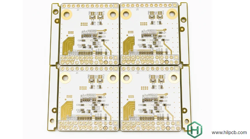
A white FR4 PCB is a glass-epoxy circuit board finished with white solder mask, usually selected when the board surface contributes to light collection, diffusion or product appearance. A production specification must control performance after assembly—not merely call the color “white.”
Key Takeaways
- FR-4 is the dielectric structure; white solder mask creates the optical surface. Specify them separately.
- Reflectance depends on wavelength, geometry, texture, formulation, thickness and cure. One percentage without a test method is incomplete.
- Qualify reflectance and color after the released reflow, cleaning and aging sequence.
- White mask does not make FR-4 thermally conductive. Select FR-4, metal-core or ceramic from the LED heat path.
- Release cosmetic zones and correlate board data with a production-intent optical fixture.
What Makes a White FR4 PCB Different
“White PCB” normally describes solder-mask color, not a special laminate. Copper circuitry is fabricated on FR-4, then a photoimageable or other specified mask is patterned. White pigments scatter visible light, but resin, fillers, cure and finish determine the result.
Optical efficiency and cosmetic whiteness differ. A backlight may prioritize spectral reflectance and uniformity; a visible board may prioritize color and gloss. One commercial mask reports greater than 85% reflectivity after reflow for its specific formulation—not a universal white-PCB value.
Specify Reflectance as Measured Data
Define the wavelength range that matters to the selected LEDs. Request a supplier curve or measured coupon rather than assuming a visible-spectrum average predicts system output.
An actionable requirement identifies:
- instrument, measurement geometry, reference and wavelength interval;
- initial and post-assembly reflectance;
- gloss or diffuse finish;
- locations, panel sampling and lot acceptance;
- color coordinates or color-difference limit when appearance matters;
- allowed within-board and board-to-board variation.
Gloss may favor directional reflection; a diffuse surface may favor angular uniformity. Validate the complete optical assembly.
Control Reflow Yellowing and Color Shift
Mask chemistry, cure, finish, flux, cleaning and repeated reflow can change white surfaces. Pink or violet discoloration has also been reported for some ENIG and mask combinations, so finish compatibility belongs in qualification.
Use the released thermal passes and profile. Compare pre- and post-assembly reflectance/color, then inspect for stains, cracks, blisters and adhesion loss. Add application-specific UV, heat, humidity or chemical aging instead of copying an unrelated hour claim.
Choose FR4 or a Better Thermal Substrate
White mask redirects light; it is not the primary heat path. Estimate junction temperature from LED power, package data, copper, dielectric, interfaces, heat sink, airflow and ambient conditions.
| Construction | Best fit | Main trade-off | Release evidence |
|---|---|---|---|
| White-mask FR-4 | Moderate heat, multilayer routing or cost sensitivity | Through-thickness thermal resistance | Thermal model and fixture test |
| Thermally enhanced FR-4 | More spreading with routing flexibility | Properties and availability vary | Named laminate data and build validation |
| Metal-core PCB | Strong one-sided heat path | Fewer routing options; dielectric is critical | Thermal resistance, isolation and stack drawing |
| Ceramic PCB | High temperature, insulation or thermal need | Cost and mechanical behavior | Exact ceramic, metallization and attachment qualification |
Choose the substrate from verified junction-temperature margin, not the presence of LEDs or an optimistic via-array assumption.
Design the Board for Light and Assembly
Reduce shadowing from tall components, dark markings, exposed copper and connectors inside the optical cavity. Keep required markings readable without placing large dark legends beside emitters. Confirm manufacturable mask dams around fine LED pads.
Balance copper for electrical, thermal and soldering needs. Asymmetry can change paste heating; removing copper for appearance can worsen heat spreading. Filled via-in-pad is package- and process-dependent, not a default.
White boards expose scratches, routing debris and residue. Define optical/cosmetic zones and stage-specific handling, cleaning and acceptance criteria.
Build an Optical Qualification Matrix
This matrix makes “high-reflectance white” auditable.
| Gate | Sample condition | Measurement | Release question |
|---|---|---|---|
| Incoming | Supplier coupon or bare board | Spectral reflectance and specified color/gloss | Does the named mask meet baseline? |
| Fabrication | Boards across panel and lot | Registration, coverage, cure, appearance and variation | Is the process repeatable? |
| Assembly | After each production-intent reflow/clean | Optical change, adhesion and defects | Does assembly damage the surface? |
| Optical build | LEDs, optic and enclosure | Output, uniformity, hot spots and color | Does board performance translate to product? |
| Reliability | Released environmental exposure | Optical drift, cracking, blistering and adhesion | Does it remain acceptable? |
Record mask product or approved equivalent, finish, laminate, copper pattern, cure route and assembly profile. Requalify after material substitution, finish/profile change or significant optical-stack revision.
Diagnose Common White PCB Failures
| Symptom | Likely cause | Evidence | Corrective direction |
|---|---|---|---|
| Yellow after reflow | Chemistry, excess heat or incomplete cure | Profile and before/after color data | Qualify mask, cure and profile together |
| Pink/violet near finish | Mask-finish interaction or contamination | Location map, finish lot and supplier analysis | Test compatible combinations |
| Uneven brightness | Texture, optics, spacing or LED variation | Reflectance and assembled light maps | Separate PCB, LED and optic effects |
| Scratches or stains | Handling, debris, flux or residue | Process-stage inspection | Improve protection and cleaning |
| Hot LED despite white board | Inadequate heat path | Junction estimate and temperature correlation | Redesign copper, dielectric, substrate or sink |
White FR4 PCB RFQ Checklist
Fabrication: Gerber/ODB++/IPC-2581, stackup, laminate, thickness, copper, finish, named mask or performance specification, texture, legend, panel and cosmetic zones.
Optical: LED parts/spectra, wavelength range, measurement method/reference, minimum and uniformity limits, color/gloss limits, locations and golden sample.
Assembly: BOM, centroid, stencil, thermal cycles/profile, flux/cleaning, handling, inspection and repair limits.
Validation: optic/enclosure, thermal budget, service exposure, output/uniformity targets, aging, sampling, traceability and requalification triggers.
Include these items with a turnkey PCB assembly request.
Reference Standards and Responsibility Boundaries
- IPC-SM-840 — IPC
- IPC-A-600 — IPC
- IPC-A-610 — IPC
- J-STD-001 — IPC
- IPC-2221 — IPC
Use contractually specified revisions. HILPCB can build to approved files and perform agreed inspection or coupon tests. The product owner remains responsible for photometry, junction temperature, environmental qualification, electrical safety, EMC and final regulatory compliance.
How HILPCB Supports White FR4 Builds
HILPCB can review the stackup, mask/finish combination, measurement plan, LED profile and inspection criteria. For greater thermal load, compare FR-4 with metal-core PCB using the real heat-flow requirement.
Start with a named mask or measurable requirement plus a production-intent golden sample. This prevents a visually white board from passing incoming inspection but failing after reflow or inside the optic.
FAQ
Is a white FR4 PCB made from white FR4 laminate?
Usually no. Glass-epoxy FR-4 forms the dielectric structure, and white solder mask creates the visible surface. Specify laminate and optical properties separately.
What reflectance should a white PCB achieve?
There is no universal value. Define wavelength range, geometry, texture, process condition and post-reflow limit. Compare named materials with the same method and validate the optical assembly.
Does white solder mask improve heat dissipation?
It does not replace a designed path through copper, dielectric, vias, substrate, interfaces and heat sink. Verify LED junction temperature from the complete thermal stack.
How can white solder-mask yellowing be prevented?
Qualify a formulation for the finish and application, control cure and reflow, use compatible flux/cleaning chemistry, and measure color or reflectance after assembly and required aging.
Conclusion
A reliable white FR4 PCB specification separates optical, thermal, cosmetic and assembly requirements. Send HILPCB optical limits, LED/optic stack, thermal budget, fabrication package and assembly profile for an evidence-based quote.