
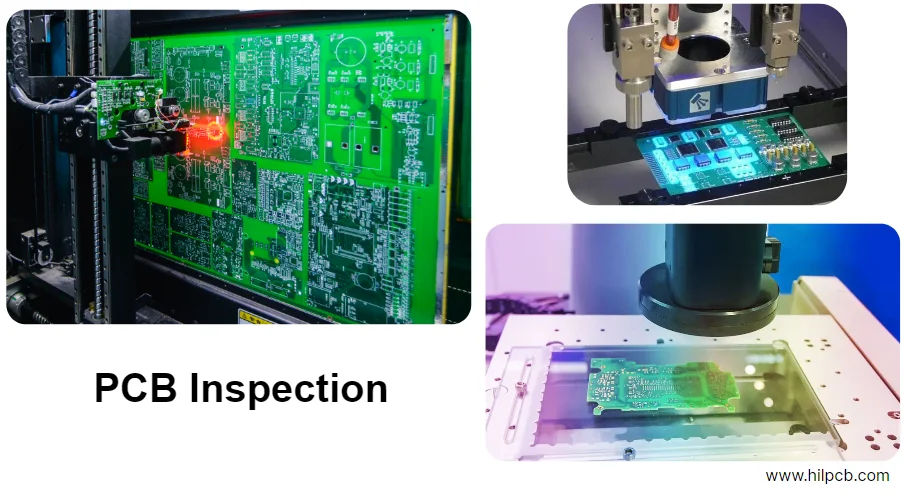
1. Executive summary: quality data-driven e KPI
Su prodotti high-frequency/high-speed/high-density, la PCB determina performance e reliability. Per HILPCB l’eccellenza nasce da misurazione, monitoraggio continuo e miglioramento sistematico. Il tema centrale—process capability analysis pcb—serve a trasformare tutto questo in KPI e pratiche operative.
KPIs principali:
- FPY: bare board > 99.5%, PCBA > 99.2%.
- CPK: su trace/space, drilling accuracy, impedance: CPK ≥ 1.67.
- OTD: multilayer standard > 98%.
Il whitepaper mostra come capability data, quality tools, test strategy e traceability end‑to‑end generano valore—con SPC/MSA, SMT/test practice e checklist DFM/DFT/DFR.
2. Core manufacturing capability: precisione e stabilità misurate
Process capability confronta le specs cliente con la variazione reale. Un PCB manufacturing whitepaper credibile deve essere data‑backed.
HILPCB key process capability metrics (mass production)
| Process step | Key capability | Performance metric | Mass production case |
|---|---|---|---|
| Innerlayer imaging | Min. trace/space | 2.5/2.5 mil (63.5/63.5 µm) | CPK > 1.67 |
| Drilling | Min. mechanical drill | 0.15 mm (6 mil) | Hole position accuracy: ±25 µm |
| Plating | Max. aspect ratio | 18:1 | Copper uniformity: >90% |
| Impedance control | Impedance tolerance | ±5% (typ.), ±3% (limit) | TDR pass rate > 99.9% |
| Solder mask | Min. solder mask dam | 3 mil (76.2 µm) | Registration accuracy: ±35 µm |
| Surface finish | ENIG | Au: 1–3 µ" / Ni: 120–240 µ" | Salt spray > 48 hours |
| Lamination | Max. layer count | 40 layers | Layer-to-layer registration: ±50 µm |
Fondamentali: gerber data preparation corretta e controllo equipment. Esempio: soldermask con LDI e best practices (soldermask exposure tutorial) per garantire precisione.
3. Toolbox qualità: closed loop (prevenzione → miglioramento)
- SPC su parametri chiave, 24/7.
- CPK su 100+ caratteristiche (base di process capability analysis pcb).
Capability highlight: CPK > 1.67 Indica bassa deriva del processo e una distribuzione (6σ) ben dentro la tolleranza. Teoricamente < 3.4 DPMO (Six Sigma).
- MSA (Gage R&R) per AOI/X-Ray/TDR.
- 8D per problem solving strutturato.
- Digital dashboard per SPC/OEE/FPY.
4. SMT/assembly capability: defect control e yield
Linee SMT (es. Fuji NXT III) per 01005 e 0.35 mm pitch BGA.
Controlli chiave: 3D SPI, placement vision, reflow profiles, 3D AOI + X-Ray (BGA/QFN). Obiettivo: una yield improvement roadmap continua.
5. Full-stack test coverage
| Test method | Description | Coverage scope | Defects detected | Applicable products |
|---|---|---|---|---|
| AOI | Image‑based inspection. | 100% SMT joints, polarity, wrong/missing parts. | Bridging, solder balls, tombstoning, offset. | All SMT assemblies |
| ICT | Probe‑based electrical test. | R/C/L, diode/transistor, opens/shorts. | Wrong values, cold joints, opens/shorts. | Mid/high-density boards |
| FCT | End‑use emulation. | I/O, interfaces, power, logic. | Design issues, firmware bugs, drift. | Function‑critical products |
| Hipot Test | High‑voltage insulation test. | Power/HV circuit insulation. | Breakdown, clearance issues, leakage. | Power/industrial/medical |
| Reliability test | Environmental stress. | Temp cycling, vibration, shock, salt spray. | Early failures, fatigue, margin issues. | Automotive/aerospace/outdoor |
Seguendo la hipot test procedure e bilanciando costi/coverage.
6. Traceability end-to-end
Serial ID per panel/unit, binding con lots materiali, parametri macchina, operator IDs, log ICT/FCT e data lake per analisi rapida—motore di miglioramento per process capability analysis pcb.
7. Checklist DFM/DFT/DFR (co-design)
HILPCB collaborative checklist (V2.0)
| Category | Check item | Best practice / recommendation |
|---|---|---|
| DFM (Manufacturing) | Gerber Data Preparation | Provide RS-274X or ODB++ with clear layer definitions. |
| Trace/space | Avoid absolute limits; keep at least 10% design margin. | |
| Pad design | Use NSMD for BGA pads; recommended pad size is 80–85% of ball diameter. | |
| Via type | Prefer through vias; use blind/buried vias cautiously. For VIPPO, specify fill and capping requirements clearly. | |
| Solder mask bridge | Ensure sufficient solder mask dam for dense pins (e.g., QFP), recommended ≥ 3.5 mil. | |
| Silkscreen | Do not print on pads; character height ≥ 30 mil; line width ≥ 5 mil for readability. | |
| Panelization | Use V-cut or mouse-bites; provide clear panel drawing; keep edge clearance (≥ 5 mm). | |
| Plane-to-pad clearance | Keep ≥ 8 mil between planes and non-connected pads/holes to avoid shorts. | |
| Fiducial marks | Place 2–3 fiducials on panel/unit diagonals; 1 mm diameter, 2 mm soldermask opening. | |
| Annular ring | Ensure adequate annular ring for all PTH (≥ 4 mil) to prevent opens. | |
| ... (15+ more items) | ... | |
| DFT (Test) | Test points | Provide ≥ 0.8 mm diameter test points for critical signals; spacing ≥ 1.5 mm. |
| Test-point distribution | Distribute points evenly; avoid crowding in one area. | |
| ICT accessibility | Do not place points under large components or within 3 mm of the board edge. | |
| JTAG/Boundary Scan | Break out TCK, TMS, TDI, TDO, TRST for JTAG-enabled ICs. | |
| Programming interface | Reserve ISP/SWD or similar for firmware programming and debug. | |
| Power isolation | Add 0Ω resistors or jumpers to isolate power domains for test. | |
| ... (5+ more items) | ... | |
| DFR (Reliability) | Component selection | Avoid EOL or single-source components. |
| Thermal management | Add thermal vias under high-power devices and increase ground copper area. | |
| Decoupling capacitors | Place close to IC power pins per datasheet recommendations. | |
| ESD protection | Add ESD devices near external ports (USB, HDMI, etc.). | |
| Material selection | Select laminates based on frequency, temperature, and environment (e.g., FR-4 TG170, Rogers). | |
| ... (5+ more items) | ... |
8. Case study & next step
Caso medical diagnostics: PCBA FPY < 90% per BGA intermittenti → analisi X-Ray/cross‑section, correzione VIPPO, vacuum reflow + 100% 3D X-Ray. Risultato: FPY 99.6%, field failures -85%.
Upload Gerber + BOM → report DFM/DFT gratuito in 24h.
FAQ
Che cosa dice davvero una process capability analysis a un team PCB o PCBA?
Indica se un processo produttivo riesce a rimanere in modo ripetibile entro i limiti di specifica invece di passare solo qualche campione occasionale. In pratica aiuta il team a capire se foratura, stampa della pasta, placement, reflow o altri passaggi critici sono abbastanza stabili per una scalata affidabile.
Perché un buon numero di yield da solo non basta a dimostrare la capability del processo?
Perché un singolo risultato di yield mostra solo cosa è successo in un lotto, mentre la capability analysis misura se il processo resta centrato e controllato nel tempo. Una linea può dare un buon rendimento nel breve periodo e comunque stare già andando verso futuri difetti se variazione, disciplina di setup o comportamento dei materiali non sono davvero sotto controllo.
Quali fasi meritano più spesso una capability analysis nella produzione elettronica?
Le fasi più importanti sono quelle che influenzano direttamente adattamento meccanico, qualità di saldatura, affidabilità elettrica o ripetibilità, come stampa della solder paste, accuratezza pick-and-place, stabilità del reflow, foratura, placcatura, controllo d'impedenza e dati critici di ispezione. Il valore è massimo quando l'analisi si concentra sui processi che impattano sia lo yield sia l'affidabilità a valle.
Come dovrebbe collegarsi la capability analysis con DFM, DFT e miglioramento continuo?
Dovrebbe essere usata come un ciclo di feedback, non come un report qualità separato. I dati dovrebbero influenzare tolleranze di progetto, strategia dei fixture, copertura di test, decisioni sulle process window e azioni correttive, così prodotto e linea produttiva migliorano insieme invece di reagire solo dopo la comparsa dei difetti.
Conclusion
Questo whitepaper copre process capability analysis pcb: CPK, yield, quality tools, test coverage e traceability, con checklist DFM/DFT/DFR. Coinvolgere presto il team DFM/DFA di HILPCB accelera prototipi e volume mantenendo quality e compliance.
Supporto manufacturing/assembly: HILPCB Turnkey Assembly o SMT Assembly.