
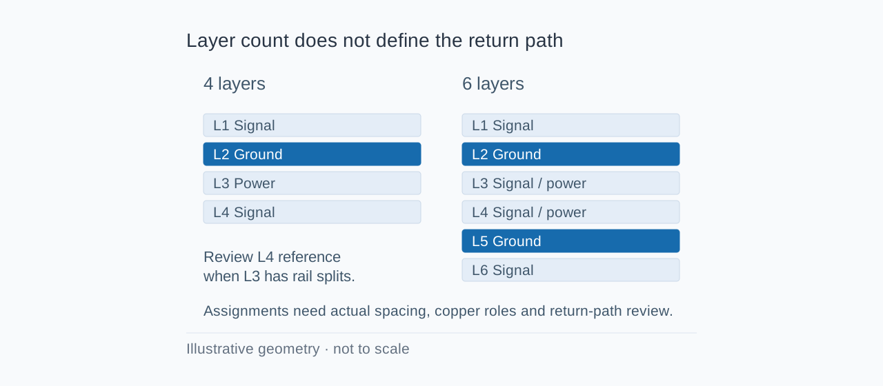
Choose four or six layers by checking whether the required routes have suitable reference planes, achievable geometries and enough routing space. Six layers can provide more routing and plane options, but the layer count alone does not establish impedance control or signal integrity.
Start with the PCB impedance and stackup workbench to compare constructions and signal-layer choices. Treat its candidates as planning inputs until the fabricator confirms cured dielectric thicknesses, materials, copper and tolerances.
When is a four-layer board a reasonable starting point?
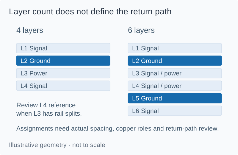
A four-layer board can work well when placement and routing allow the important signals to stay near continuous references and the power distribution fits the remaining copper. A common starting assignment is L1 signal, L2 ground, L3 power and L4 signal.
That shorthand hides a key review question: L4 is adjacent to L3. If L3 is split into several rails, a bottom route can cross a reference discontinuity. Even a continuous power plane needs an appropriate AC return connection to ground when a signal transition changes reference. Calling every internal copper layer a ground plane in a calculator does not make it one physically.
Another four-layer approach uses ground on both inner layers and distributes power with outer-layer copper. It can give both outer signal layers a ground reference, at the cost of routing and power-distribution space. Compare the actual copper roles and placement rather than assuming one assignment is universally best.
What can six layers add?
An illustrative six-layer assignment is L1 signal, L2 ground, L3 signal/power, L4 signal/power, L5 ground and L6 signal. Both outer layers can then be adjacent to ground, while additional internal copper can help with routing and power distribution.
The middle layers still require a physical cross-section review. Their relationship to both ground planes, each other and any power regions depends on the dielectric spacings and copper patterns. Do not assume that every L3/L4 route behaves as an isolated stripline merely because the board has six layers. Nearby signal copper can create coupling.
| Review question | Four-layer route to acceptance | Reason to investigate six layers |
|---|---|---|
| Can critical routes keep a continuous reference? | Place and route them on layers adjacent to suitable planes | Existing assignments force repeated plane splits or reference changes |
| Can the target width and pair gap be fabricated? | Confirm suitable trace-to-plane dielectric and realistic copper | Another construction provides more practical geometry |
| Is there enough routing space? | Resolve placement and escape congestion without long detours | Extra routing layers reduce density pressure |
| Can power paths meet drop and thermal budgets? | Use adequate pours/planes and connected via arrays | Additional copper allocation helps distribution |
| Are the stack and copper distribution practical to build? | Confirm symmetry, material availability and finished thickness | A revised symmetric construction better suits the design |
Worked planning example: total thickness is not reference height
Suppose two proposed boards are both 1.60 mm thick. Candidate A places the L1 reference plane 0.10 mm below the signal layer. Candidate B places it 0.20 mm below that layer. Both use an illustrative 0.20 mm signal width.
| Parameter | Candidate A | Candidate B |
|---|---|---|
| Overall thickness | 1.60 mm | 1.60 mm |
| Trace-to-reference dielectric height h | 0.10 mm | 0.20 mm |
| Trace width w | 0.20 mm | 0.20 mm |
| Geometric ratio w/h | 2.0 | 1.0 |
The electrical cross-sections are different even though overall thickness is identical. For a common single-ended microstrip with the other inputs fixed, increasing reference height increases impedance. The table deliberately does not assign either candidate a 50 Ω result: copper thickness, material Dk, mask and the selected model still need to be specified and calculated.
These spacings are hypothetical planning examples, not stocked laminations or a fabrication offer. Ask the supplier for its proposed cured stack, then use that construction for the calculation. See the impedance calculator guide for the input and tolerance workflow.
How should you compare candidates in the workbench?
- Enter the candidate layer count, board thickness and nominal copper, then apply the board settings.
- Add the actual single-ended or differential requirements, including target impedance and signal layer.
- Review the upper and lower references. A nearby copper layer is a reference only when the physical geometry and electrical connection support that assumption.
- Use Trace width from target impedance to explore width, or Impedance from current geometry to check a routed width and gap.
- For a differential pair, choose whether synthesis keeps edge gap or center pitch fixed. They describe different geometric constraints.
- Review section parameters and the physical stack, including explicit coating and intervening copper roles where applicable. Resolve unknown geometry before using the result.
- Compare viable candidates with the fabricator, including process tolerances and which artwork changes require your approval.
Check input definitions before changing layer count. Include plane splits and nearby copper when deciding whether a candidate meets its requirements.
What else belongs in the comparison?
The trace-width calculator helps check current, resistance and drop. A six-layer stack does not automatically remove a narrow power neck-down. The via-current guide explains the separate layer-transition check.
More layer changes can also introduce via discontinuities. The via inductance and via capacitance tools provide geometry comparisons; neither replaces a full transition model. A good stackup can reduce unnecessary transitions through better layer assignment.
What should you send for stackup review?
Include the layer-role drawing, overall thickness and tolerance, required impedance structures, material preferences, minimum copper, critical current paths and via construction. Mark reference-plane continuity and any intentional voids. Define whether the supplier may change trace width, gap or dielectric construction and how substitutions are approved.
For controlled impedance, agree the representative coupon, test method and acceptance band. IPC-TM-650's published test methods include characteristic-impedance measurement guidance. General return-path considerations are discussed in TI's High-Speed Layout Guidelines. Use the project-required standard editions and supplier-confirmed production stack.
FAQ
Are six layers always better than four?
No. Six layers offer more allocation options, but placement, reference continuity, dielectric spacing and implementation determine whether those options help.
Can a four-layer PCB have controlled impedance?
Yes, when the selected construction and geometry support the targets and the fabrication/test requirements are agreed. Layer count alone is not the deciding criterion.
Does a 1.6 mm board need 1.6 mm entered as microstrip height?
No. Microstrip height is the relevant trace-to-reference spacing, as defined by the model. Total board thickness is a different dimension.
Should I choose layer count from clock frequency alone?
No. Also consider edge rate, return paths, routing density, power distribution and the complete interface requirements. A relatively slow clock can still have fast edges.
Compare a four-layer and six-layer candidate, then request a PCB quote with the intended references and impedance requirements attached.