
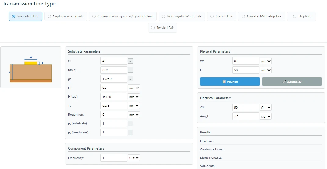
An online PCB impedance calculator estimates a transmission line's characteristic impedance from its cross-section, dielectric properties, conductor data, and frequency inputs. Use it to explore geometry before layout—not to replace the fabricator's production stackup, field-solver review, or TDR acceptance test.
Key Takeaways
- Select the model that matches the physical structure; microstrip, stripline, coplanar, and coupled traces are not interchangeable.
- Use cured dielectric thickness, finished copper, and construction-specific Dk rather than nominal board thickness or generic “FR-4 = 4.4.”
- Run nominal, low-limit, and high-limit inputs to see whether manufacturing variation consumes the impedance tolerance.
- Differential impedance depends on both traces, their spacing, references, and surroundings; it is not always twice the isolated single-ended value.
- Treat the calculator result as a design starting point. The factory must return manufacturable geometry and verify the contracted coupon.
How Do You Use the HILPCB Impedance Calculator?
Open the HILPCB online impedance calculator, choose the transmission-line type, enter the geometry and material inputs, then analyze the result. The current interface includes microstrip, coupled microstrip, stripline, coplanar waveguide with and without a lower ground plane, coaxial line, rectangular waveguide, and twisted pair models. PCB designers will most often use the microstrip, coupled-microstrip, stripline, and coplanar options.
Use Analyze when width, spacing, dielectric height, copper thickness, Dk, and frequency are known. Use Synthesize to explore a geometry for a target impedance, then check that the proposed dimensions remain manufacturable. Available outputs vary by model and can include impedance, effective permittivity, propagation delay, conductor/dielectric loss estimates, electrical length, and skin depth.
Which Inputs Matter Most?
| Input | Typical effect when increased | Production detail to use |
|---|---|---|
| Trace width | Lowers characteristic impedance | Finished etched width, not only CAD width |
| Dielectric height to reference | Raises impedance in common microstrip geometries | Cured prepreg/core thickness |
| Relative permittivity, Dk | Lowers impedance | Construction- and method-specific design Dk |
| Copper thickness | Often lowers impedance modestly | Finished copper after plating where applicable |
| Differential-pair gap | A smaller gap usually lowers differential impedance | Manufacturable edge-to-edge spacing |
| Solder mask / upper dielectric | Changes outer-layer effective permittivity | Model coating only when the selected structure supports it |
| Frequency, Df, roughness | Affect loss and dispersion estimates | Values defined by frequency, method, foil side, and material construction |
These directions are useful for intuition, not a substitute for the selected model. Nearby copper, plane voids, trapezoidal etch, glass weave, roughness, and solder mask can make the real cross-section differ from the ideal drawing.
What Is the Three-Pass Sensitivity Check?
Do not record only one impedance number. Run three cases:
- Nominal: the fabricator's proposed production geometry and material values.
- Low-impedance corner: combine plausible variables that push impedance downward, such as wider trace, thinner dielectric, or higher Dk.
- High-impedance corner: combine plausible variables that push it upward, such as narrower trace, thicker dielectric, or lower Dk.
| Result | Design decision |
|---|---|
| All three runs remain inside the requirement | Proceed to fabricator review and coupon definition |
| A corner fails but geometry has room | Adjust width, gap, dielectric construction, or tolerance allocation |
| Small input changes create large shifts | Use a more robust geometry or tighter controlled process |
| Calculator and fabricator disagree | Compare model, Dk basis, copper definition, mask, and cured thickness before changing artwork |
This check does not calculate statistical yield, but it exposes fragile assumptions before routing is frozen.
When Is an Online Result Not Enough?
Use a fabricator's controlled stackup and suitable field solver for fine geometry, asymmetric structures, broadside or coplanar coupling, unusual coatings, multiple dielectrics, high-frequency loss, or transitions involving vias and connectors. No 2D trace calculator proves a complete channel.
For production, define an impedance coupon that represents the relevant layer, copper process, dielectric construction, geometry, and mask condition. IPC-TM-650 2.5.5.7 describes TDR measurement of characteristic impedance. A coupon pass verifies the contracted coupon; it does not certify every BGA escape, via, connector, or full protocol channel.
What Should the Controlled-Impedance RFQ Include?
- fabrication data, netlist, layer order, reference planes, and finished thickness
- nominal impedance and tolerance for each single-ended or differential structure
- layer, routing model, mask condition, target width/gap, and whether the factory may adjust geometry
- exact or approved laminate construction, Dk basis, copper weight/profile, and substitutions
- coupon correlation, TDR method, sampling, report format, and acceptance criteria
- quantities, panel/array needs, applicable IPC revision/class, deviation approval, and change notice
HILPCB can review the stackup and controlled-impedance package for a multilayer PCB. Actual trace geometry, tolerance, material, coupon, test evidence, and lead time must be confirmed in the quotation.
Standards and Responsibility Scope
Common references include IPC-2141A for controlled-impedance design guidance, IPC-2221C for generic printed-board design, IPC-6012E for rigid-board performance when invoked, and IPC-TM-650 2.5.5.7 for TDR measurement.
The customer owns interface targets, architecture, simulation, and system validation. HILPCB owns only the fabrication, review, coupon, inspection, and test scope accepted in writing. Calculator output is not a product-performance or compliance guarantee.
Common Questions
Is an online PCB impedance calculator accurate enough for production?
It is useful for planning and sensitivity analysis. Production geometry should come from the selected factory's stackup and be verified with the agreed coupon and test method.
Should I enter total board thickness as dielectric height?
No. Enter the dielectric distance from the trace to its relevant reference plane or planes, as defined by the selected transmission-line model.
Why does the fabricator return a different trace width?
The factory may use different cured thickness, Dk, finished copper, etch compensation, mask, or solver assumptions. Compare inputs and model definitions before approving the change.
Does 100-ohm differential impedance mean two 50-ohm traces?
Not necessarily. Coupling changes odd-mode impedance, so differential impedance depends on pair spacing and the complete cross-section.
Use the calculator to build a defensible starting geometry, then submit the controlled-impedance package to HILPCB for construction-specific review and quotation.