
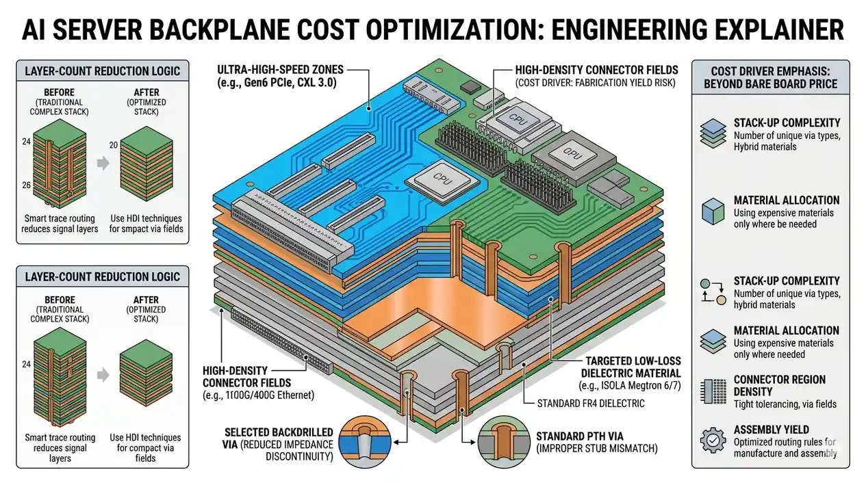
AI Server Backplane Cost Optimization: Cost Drivers, DFM Levers, and Pre-RFQ Release Checklist
Optimizing the cost of an AI server backplane is not about negotiating the bare-board unit price. True cost reduction comes from controlling the five parameters that drive 78–85% of total board cost: layer count, laminate grade, HDI microvia structure, impedance control and backdrilling, and yield loss. A cost strategy that ignores these levers and focuses only on supplier margin will defer penalties into pilot-run scrap, SMT rework, and schedule slips that cost more than any unit-price savings.
This guide helps hardware engineers, NPI teams, and procurement buyers make three decisions: which cost levers produce authentic savings, which specifications to lock before releasing the RFQ, and which over-design patterns to audit before tape-out.
What Drives AI Server Backplane Cost?
An AI server backplane simultaneously routes PCIe 5.0/6.0, CXL, inter-switch links, management buses, and high-current power distribution across 20–44 layers at 3.2–6.4 mm thickness. The cost structure is dominated by five drivers:
AI Server Backplane Cost-Driver Breakdown
| Cost Driver | Share of Board Cost | Primary Lever | Risk of Over-Compression |
|---|---|---|---|
| Layer count (20–44 layers) | 28–35% | Floor-plan optimization; connector fan-out review | SI degradation; warpage; SMT yield collapse |
| Advanced laminates | 22–30% | Zoned material use; hybrid stackup | Channel loss budget exhaustion; respin |
| HDI microvia structures | 15–20% | Limit any-layer to connector zones | Lamination cycle complexity; reliability risk |
| Impedance control + backdrilling | 10–15% | Surgical backdrill scope; tiered impedance tolerance | Return loss resonance on critical links |
| Yield loss | 8–14% | Copper balance; panel utilization; DFM review | Scrap; lead-time escalation; rework cost |
For context, an AI server backplane panel in Megtron 7 costs approximately 6–8× an equivalent FR-4 traditional server backplane panel, and a finished AI server board typically ranges from $900 to $1,800+ per board versus $80–$150 for a standard 1U/2U server board.
Why Is Layer Count the Largest Cost Lever?
Adding two layers is not just two sheets of foil and prepreg — it means additional core boards, more complex lamination press cycles, extended plating duration, and higher AOI scrap sensitivity. Reducing a 24-layer design to 22 layers, or a 32-layer design to 28 layers (a documented ~12.5% cost savings), is the single most direct cost lever available.
However, layer reduction is only valid if the compressed stackup still supports:
- Routing density for all connector fan-out paths without detours
- Continuous reference planes for every high-speed differential pair
- Clean power delivery planes without split regions
- Z-axis symmetry to prevent post-lamination warpage (typically < 0.5% for SMT)
- Adequate ground return vias and stitching for crosstalk suppression
The engineering questions to answer before approving layer reduction:
- Are current layers bloated because poor floor-planning forced cross-board routing detours?
- Do connector placements arbitrarily lengthen critical channels or block fan-out?
- Can return paths, power planes, and signal routing coexist after pruning?
- Does the stackup retain Z-axis symmetry to avoid yield loss from warpage?
If the answer to any of these is uncertain, the layer reduction will transfer cost into SI validation failures and prototype respins — the opposite of optimization.
How Do You Control Laminate Cost Without Breaking the Channel?
Premium ultra-low-loss and extremely-low-loss laminates are justified only on the longest, highest-speed channels. Blanket-applying them across the entire board is a common false-savings pattern: it inflates the laminate line item (22–30% of cost) without improving performance on short or low-speed nets.
Laminate Grade Cost Index and Application Window
| Material Grade | Df @ 10 GHz | Cost Index (FR-4 = 1×) | Application Window |
|---|---|---|---|
| Standard FR-4 | 0.018–0.022 | 1× | Low-speed sideband, power, mechanical layers |
| Mid-loss | 0.010–0.015 | 2–3× | Medium-speed transit; management buses |
| Low-loss | 0.005–0.008 | 4–6× | PCIe 4.0/5.0 short channels; CXL 2.0 |
| Ultra-low-loss | 0.003–0.005 | 8–12× | PCIe 5.0 long channels; 112G PAM4 |
| Extremely-low-loss | < 0.003 | > 15× | 224G PAM4; longest SerDes channels |
A hybrid stackup uses premium cores only on the specific high-speed signal layers, with mid-loss or standard FR-4 on power and low-speed layers. This requires verifying supply chain stability for the premium laminate and confirming that its flow characteristics under high-pressure lamination are repeatable across batches. Cross-reference the design against 112G SerDes routing constraints and 112G stackup and channel budgets to determine exactly when a material upgrade protects total cost.
Why Must Backdrilling Be Surgically Deployed?
Backdrilling is a notorious cost multiplier. It is essential for truncating via stubs on high-speed channels — a 5.5 mm via stub resonates at approximately 7 GHz, and the Bogatin rule requires stubs under 12 mil for 25 Gbps NRZ — but defaulting to "backdrill everything" exponentially escalates CNC machining time, drill bit consumption, and impedance-controlled QA verification.
Backdrilling should be applied only to:
- The highest-speed critical differential links
- Long channels forced to traverse multiple internal core layers
- Dense connector fan-out zones where via-stub resonance breaks reflection limits
- Paths where top-layer routing alone cannot salvage the loss budget
The cost adder for backdrilling is typically 5–10% on a high-layer-count build. Grouping backdrill depths and sharing drill programs across similar vias reduces this adder. The engineering question is not "Can we backdrill this?" but "Does backdrilling this specific via mathematically save the channel?" For detailed process guidance, see Backdrill PCB process controls.
How Do Connector Zones Dictate Backplane Cost?
The connector arrays are where electrical and manufacturing bottlenecks converge. High-density orthogonal or backplane connectors impose restricted anti-pad clearances, extreme drill-hole density, paralyzing fan-out blockades, and competition for localized layer resources. If connector part numbers, pin-out maps, or press-fit parameters are frozen late, the layout team can only salvage the board by adding layers, expanding backdrilling, or accepting poor yields.
Practical cost reviews proactively confirm:
- Has the dense connector zone already exhausted layer routing real estate?
- Do localized vs. global copper balance disparities guarantee post-bake warpage?
- Does the large-format panel present mechanical deflection risks during connector mating?
- Are SMT assembly capabilities and turnkey assembly boundaries evaluated for press-fit and heavy hardware?
- Does the structural integrity warrant checking panelization design quality for large-format handling?
What Should You Lock Before Releasing the RFQ?
The following pre-RFQ release checklist defines what must be frozen, who owns the decision, and the risk of leaving it fluid. This is the single most effective cost-optimization action because it prevents downstream respins, material swaps, and yield surprises.
Pre-RFQ Release Checklist with Owner Matrix
| Item to Lock | Owner | Risk if Not Locked |
|---|---|---|
| Network tiering (high/medium/low-speed) | SI engineer | Blanket premium rules; total over-design |
| Layer count and Z-axis symmetry | Layout lead + fab DFM | Warpage; SI failure; respin |
| Material grade per layer zone | SI engineer + procurement | Laminate cost inflation; supply delay |
| Backdrill scope and depth rules | SI engineer | CNC cost explosion; QA bottleneck |
| Connector part numbers and pin-out maps | System architect | Fan-out paralysis; layer addition; yield loss |
| Impedance targets and tolerance per net class | SI engineer | TDR failure; reflow yield loss |
| Press-fit hole tolerances | Mechanical engineer + fab | Connector coplanarity failure; scrap |
| Test coupon rules and acceptance class | Quality/NPI + fab | No SI evidence; rejection at FAI |
| Panel utilization and copper balance | Fab DFM | Warpage scrap; SMT coplanarity failure |
| Surface finish and copper weight per layer | Fab DFM + procurement | Solderability issues; cost adders |
How Do You Audit for Over-Design?
Over-design is the most common hidden cost driver. Use this audit matrix to identify specifications that inflate cost without protecting performance.
| Over-Design Pattern | Cost Impact | Audit Question |
|---|---|---|
| All nets use the tightest impedance tolerance (±5%) | 10–15% impedance control premium | Can non-critical nets use ±8–10%? |
| Premium laminate on all layers | 22–30% laminate premium | Can power and low-speed layers use mid-loss? |
| Backdrill on all vias | 5–10% CNC + QA premium | Which vias have stubs > 12 mil on critical paths? |
| Any-layer HDI across entire board | 15–20% lamination premium | Can HDI be limited to connector zones? |
| All differential pairs at minimum trace/space | Yield loss; AOI scrap | Can non-critical pairs use wider spacing? |
Frequently Asked Questions (FAQ)
Q: Is downgrading the laminate the fastest way to reduce backplane cost?
A: No. In most AI server backplane designs, optimizing the layer count, connector fan-out, and backdrill scope produces a more direct cost impact than a dielectric downgrade. Any material change must stem from simulated channel budgets — downgrading a laminate on a long 112G channel will exhaust the insertion loss budget and trigger a respin that costs far more than the material savings.
Q: Does removing two layers always save money?
A: Only if the compressed stackup still supports routing density, return paths, EMI shielding, and copper balance. If pruning layers degrades SI or induces warpage, the pilot-rework costs will exceed the layer savings. A documented case showed 32 → 28 layers yielding ~12.5% savings, but only after confirming all connector fan-out paths were preserved.
Q: Why does backdrilling become a cost black hole?
A: Blanket backdrilling multiplies CNC machining time, drill bit consumption, and impedance-inspection bottlenecks. It should be reserved for high-speed differential links where via-stub resonance mathematically breaks the channel. Grouping backdrill depths and sharing drill programs reduces the cost adder.
Q: What is the single most effective cost-optimization action?
A: Freezing the pre-RFQ release checklist — network tiering, layer count, material zones, backdrill scope, connector part numbers, impedance targets, and test coupon rules — before sending the package to the fabricator. Fluid specifications at tape-out are the root cause of most downstream respins, material swaps, and yield surprises.
Next Steps
If your hardware engineering team is architecting AI servers, high-density network switches, or high-speed interconnect platforms, HILPCB provides:
- Backplane cost and DFM pre-reviews: Isolate risks in layer limits, material matching, backdrilling tolerances, connector densification, and SMT yield before routing release → Explore PCB manufacturing and full DFM support
- Stackup and high-speed material synchronization: Formulate cost-to-performance matrices aligned with channel budgets and factory specs → View high-speed PCB production capacity
- NPI prototype and mass-production scalability: Chain bare-board fabrication, advanced assembly, and First Article Inspection into a unified deliverable → Request an integrated PCB fabrication and assembly quote
To request an AI backplane cost optimization audit, a dielectric vs. layer-reduction viability analysis, or a connector DFM review before committing to first-article prototypes, connect with the PCB engineering team to define your project parameters.
Related engineering resources:
- 112G SerDes Routing Strategies: Identifying which structures cannibalize speed margins and budget.
- 112G SerDes Stackups and Budgets: How to freeze material grades, stackup alignments, and insertion bounds.
- Backdrill PCB Process Controls: Why precise, localized backdrill execution is mandatory.
- PCB Stackup Documentation Guide: How to script layer matrices, materials, and impedance bounds for the fab.
- PCB Design Handoff Best Practices: Eliminating factory data misinterpretations and pilot-run iteration loops.