
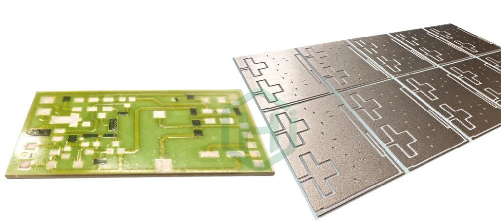
An Al₂O₃ ceramic PCB manufacturer converts alumina into a patterned circuit or metallized assembly using direct bonded copper (DBC), direct plated copper (DPC), thick film, or thin film. The supplier must match substrate, metallization, geometry, finish, assembly, and evidence to the mission profile.
Alumina combines electrical insulation, mechanical strength, mature processing, and lower cost than many higher-performance ceramics. It is not best for every high-power, RF, medical, or high-temperature design.
Key Takeaways
- Select the ceramic and metallization together; “Al₂O₃ PCB” alone does not define the construction.
- A representative 96% alumina datasheet lists about 24 W/m·K thermal conductivity; use the purchased grade’s certified value.
- DBC suits relatively thick copper and power paths; DPC supports finer plated features; thick film enables printed conductors and resistors. These processes are not interchangeable.
- DBC bonding or thick-film firing temperature does not define finished-PCBA operating temperature.
- Thermal performance follows the junction-to-coolant path; reliability follows copper/ceramic stress, geometry, attachment, and cycle profile.
- Put material certificates, dimensional limits, inspection, electrical test, adhesion or thermal-cycle evidence, assembly scope, and acceptance criteria into the RFQ.
Table of Contents
- What is an Al₂O₃ ceramic PCB?
- When should alumina be chosen instead of AlN or another substrate?
- Which metallization process should be used?
- What should be specified before quotation?
- What causes alumina ceramic circuits to fail?
- Which supplier evidence should buyers request?
- How should ceramic PCB assembly be planned?
- What drives cost and lead time?
- What should an Al₂O₃ PCB RFQ include?
What Is an Al₂O₃ Ceramic PCB?
An alumina PCB is an aluminum-oxide circuit carrier. The ceramic provides insulation and support; metallization creates conductors, pads, resistors, vias, or attachment surfaces. Unlike FR-4, it has no woven glass-reinforced organic dielectric.
Common grades include 96% and higher-purity alumina. Properties vary by formulation, porosity, thickness, finish, and supplier. CeramTec publishes 24 W/m·K thermal conductivity and 15 kV/mm dielectric strength for one 96% Rubalit grade; these are reference points, not universal values.
“Stable above 800°C” is misleading. Process firing or bonding may exceed 800°C, but finished circuits contain copper, plating, attach materials, components, encapsulants, and interfaces. The lowest qualified element and mission profile set service temperature.
Applications include power modules, LED/laser submounts, heaters, sensors, hybrid circuits, and isolation structures. Suitability still requires system-level electrical, thermal, mechanical, safety, and regulatory validation.
When Should Alumina Be Chosen Instead of AlN or Another Substrate?
Select material from heat flux, insulation, fracture behavior, CTE compatibility, geometry, environment, availability, and cost—not a generic “ceramic is better” rule.
| Substrate | Main advantage | Main trade-off | Typical selection trigger |
|---|---|---|---|
| Alumina (Al₂O₃) | Mature, electrically insulating and cost-effective; specific 96% grades are commonly around the mid-20 W/m·K range | Lower thermal conductivity than AlN; brittle; properties vary with purity and formulation | Moderate heat flux, isolation, hybrid circuits, sensors, heaters and cost-sensitive power electronics |
| Aluminum nitride (AlN) | Much higher thermal conductivity and CTE closer to silicon in many grades | Higher cost; processing and thermo-mechanical reliability require careful review | Heat spreading dominates and alumina creates excessive thermal resistance |
| Silicon nitride (Si₃N₄) | High fracture toughness and strong thermal-cycling potential in power modules | Higher cost and a more specialized supply chain | Severe cycling or mechanical reliability dominates |
| Metal-core PCB | Familiar PCB processing and economical heat spreading for many assemblies | Organic dielectric remains in the thermal path and limits isolation/temperature performance | Heat spreading is needed without ceramic-level electrical or mechanical requirements |
| FR-4 / high-Tg PCB | Lowest-cost, multilayer routing and broad assembly ecosystem | Much lower through-thickness thermal conductivity and higher CTE | Routing density and cost dominate while heat flux remains manageable |
Thermal conductivity is one input. Estimate resistance through ceramic, copper, die attach, interface, baseplate, and cooler. Thin alumina may outperform poorly integrated AlN, while strength or dielectric requirements may set minimum thickness.
Which Metallization Process Should Be Used?
Metallization controls conductor thickness, feature size, surface, chemistry, embedded functions, and reliability. Require the exact process; “ceramic PCB” is incomplete.
| Process | How the circuit is formed | Best fit | Main review points |
|---|---|---|---|
| DBC / DCB | Copper foil is bonded to alumina or AlN at high temperature, then patterned | Power modules, thicker copper, current spreading and die attach | Copper/ceramic thickness ratio, etch geometry, edge stress, flatness, voids/delamination, surface finish |
| DPC | A seed/adhesion system is deposited and copper is plated to the required thickness | Fine features, sensors, LEDs, RF or precision submounts | Adhesion stack, plating uniformity, via fill, surface roughness, line/space and finish |
| Thick film | Conductive, resistive and dielectric pastes are printed and fired | Hybrid circuits, printed resistors/heaters, crossovers and economical prototypes | Paste system, fired thickness, sheet resistance, print tolerance, silver migration/leaching, overglaze |
| Thin film | Metal layers are deposited and patterned by photolithographic methods | Fine geometry, controlled RF structures, precision sensors and optical submounts | Adhesion/barrier layers, metal thickness, surface roughness, etch control and wire-bond finish |
| LTCC / HTCC | Conductors and vias are built into co-fired multilayer ceramic | Embedded multilayer interconnect and compact packages | Shrinkage, via/metallization system, material set, cavity geometry and qualified process ownership |
DBC is not merely “better adhesion,” nor DPC “finer DBC.” They differ in materials, thickness ranges, geometry, cost, and failure modes. Thick film can add printed resistors that DBC needs extra processing to provide.
What Should Be Specified Before Quotation?
Gerbers plus “Al₂O₃” are insufficient. Freeze these inputs or mark them for engineering review:
| Design domain | Required definition | Why it changes the process |
|---|---|---|
| Ceramic | Material grade/purity, supplier restriction, thickness, surface finish, color if relevant | Controls certified thermal, dielectric, mechanical and dimensional properties |
| Metallization | DBC, DPC, thick/thin film or co-fired route; conductor material and thickness | Determines tooling, geometry, current path, finish and attachment compatibility |
| Geometry | Outline, scribe or routed edges, holes, slots, cavities, edge metallization, datum scheme | Ceramic machining and singulation can initiate chips or cracks |
| Circuit rules | Line/space, copper clearance to edge/hole, pad geometry, vias, resistor values/tolerances | Establishes process feasibility and inspection method |
| Finish | Bare copper, silver system, ENIG, ENEPIG, nickel/gold or wire-bondable finish as applicable | Must match solder, braze, aluminum/gold wire, die attach and storage requirements |
| Thermal/mechanical | Heat sources, attachment area, baseplate/cooler, mounting load, flatness and coplanarity | Prevents a substrate-only thermal claim from replacing assembly design |
| Environment | Voltage, frequency, temperature profile, thermal cycles, humidity, vibration and chemicals | Defines insulation, corrosion, crack and attachment risks |
| Acceptance | Dimensional, visual, electrical, adhesion, microsection, SAM, thermal or reliability evidence | Converts “high reliability” into auditable requirements |
Review DBC copper balance early. Copper/ceramic expansion mismatch concentrates stress near edges. Evaluate both thicknesses, pattern symmetry, pad geometry, edge distance, and mission profile together.
What Causes Alumina Ceramic Circuits to Fail?
Failures often begin at interfaces, not in bulk alumina. Rogers highlights CTE mismatch, copper-edge stress, thickness ratio, pattern balance, and cycle conditions.
| Failure mode | Common contributors | Evidence or design response |
|---|---|---|
| Edge chip or substrate crack | Laser/machining damage, sharp mechanical load, poor support, handling | Edge criteria, magnified inspection, suitable packaging and assembly fixtures |
| Copper/ceramic delamination | Bonding/plating defect, contamination, stress, incompatible geometry | Process-specific adhesion evidence, cross-section or SAM when contracted |
| Thermal-cycle crack near copper | CTE mismatch, thick copper on thin ceramic, unbalanced pattern, aggressive cycle | Mission-profile cycling, stress-aware layout, copper/ceramic ratio review |
| Solder or die-attach fatigue | CTE mismatch across die, ceramic, baseplate and attachment | Attachment-material selection, void criteria, thermal cycling/power cycling |
| Wire-bond lift or poor bond | Wrong finish, contamination, roughness, plating thickness or storage | Finish certificate, bond pull/shear plan, cleanliness and shelf-life control |
| Silver migration or leaching | Thick-film conductor chemistry, moisture/electric field, solder process | Select suitable Ag/Pd or barrier/finish system; validate under use conditions |
| Local overheating | Thermal path not modeled, voided attach, small spreading area, cooler interface | Junction-to-coolant thermal model and measured thermal impedance |
| Dielectric breakdown | Insufficient thickness/spacing, defects, contamination, transient overvoltage | Insulation coordination, defined withstand/IR test and product safety validation |
Thermal cycling compares constructions; it does not guarantee life. Endpoints, dwell, ramp, sample, failure definition, and inspection change results. A cycle count matters only when the vehicle and profile resemble the product mission.
Which Supplier Evidence Should Buyers Request?
Distinguish capability from marketing by requesting evidence tied to the quoted construction.
| Supplier claim | Useful evidence | What it does not prove |
|---|---|---|
| “96% alumina” | Material certificate identifying grade, lot, thickness and key properties | Properties of a different supplier or purity |
| “DBC/DPC capability” | Process flow, design rules, copper range, finish options and relevant sample report | Suitability for the customer’s geometry without DFM |
| “High bond strength” | Defined peel/pull method, coupon geometry, sample plan and acceptance value | Thermal-cycle life of the complete module |
| “High-voltage ceramic” | Test method, voltage waveform, ramp, duration, environment, spacing and pass rule | Product safety certification or field insulation margin |
| “Thermal reliability” | Mission-relevant thermal/power cycling plus crack/delamination inspection and thermal-impedance data | Universal service life |
| “Medical capable” | Current QMS certificate and agreed traceability/process records | Medical-device approval, FDA clearance or product safety |
| “Full traceability” | Sample traveler/report linking material lot, process, inspection, test, assembly and shipment | Correctness of requirements not included in the traveler |
| “Turnkey assembly” | Assembly design rules, finish/attachment compatibility, inspection and test scope | System performance unless explicitly tested |
Check QMS certificates for entity, site, scope, issuer, and validity. ISO 9001 or ISO 13485 covers a management system; it does not certify a PCB or approve the final device.
How Should Ceramic PCB Assembly Be Planned?
Plan assembly around brittleness, thermal mass, finish compatibility, and heat path. Do not copy an FR-4 profile or fixture without review.
Assembly may include SMT, die attach, wire/ribbon bonding, brazing, lead attachment, baseplate joining, underfill, coating, or encapsulation. Each needs compatible metallization and finish; ENIG, ENEPIG, nickel/gold, bare copper, and silver thick film are not equivalent.
Define board support, thermal gradients, bow, attach material, void criteria, cleaning, wire/bond parameters, pull/shear sampling, rework, and interface flatness. HILPCB can review fabrication and applicable turnkey assembly, but each material/package/attachment needs confirmation.
What Drives Cost and Lead Time?
Cost follows ceramic grade/thickness, panel availability, metallization, metal thickness, print/firing steps, features, cavities, machining, finish, singulation, inspection, testing, fixtures, yield, and quantity.
Control cost with alumina where the thermal model permits, standard thicknesses, necessary tolerances, edge clearances, one compatible finish, and separate prototype versus recurring tests. Classify tests as qualification, lot acceptance, or periodic monitoring.
What Should an Al₂O₃ PCB RFQ Include?
Substrate and circuit
- Al₂O₃ grade/purity, preferred supplier if controlled, thickness, size and surface requirements
- metallization process, conductor material/thickness, layer count and required finish
- Gerber/ODB++, drawing, DXF/STEP where needed, datum scheme and revision
- line/space, edge clearance, holes, slots, cavities, scribe, via and resistor requirements
- flatness, coplanarity, chip/crack criteria, dimensional tolerances and marking
Electrical, thermal and mechanical
- operating and transient voltage, frequency, current, insulation and spacing requirements
- heat-source map, allowable temperature, cooling stack, interface material and mounting load
- operating/storage temperature profile, thermal or power cycles, humidity, vibration and chemicals
- die, package, baseplate and connector materials that affect CTE or attachment
Assembly and test
- BOM/AVL, component or die data, solder/die-attach/braze system and wire-bond material
- stencil, fixture, cleaning, coating, encapsulation, rework and handling expectations
- visual/dimensional inspection, continuity, isolation resistance and withstand-voltage details
- adhesion, bond pull/shear, X-ray, SAM, thermal impedance, thermal cycling or other contracted evidence
- FAI scope, sample plan, acceptance values, report format, traceability and record retention
Commercial and responsibility split
- prototype and production quantities, target date, partial shipment and forecast
- customer-supplied versus manufacturer-sourced material and tooling ownership
- approved substitutions, deviation authority and engineering-response contacts
- qualification, lot-acceptance, periodic and system-level tests with named owners
Standards and Responsibility Scope
References depend on construction and end product:
- IPC J-STD-001 — Requirements for Soldered Electrical and Electronic Assemblies
- IPC-A-610 — Acceptability of Electronic Assemblies
- IPC-4552 — Electroless Nickel/Immersion Gold (ENIG) Plating for Printed Boards
- IPC-4556 — Electroless Nickel/Electroless Palladium/Immersion Gold (ENEPIG) Plating
- ASTM D149 — Dielectric Breakdown Voltage and Dielectric Strength of Solid Electrical Insulating Materials
- IEC 60664-1 — Insulation Coordination for Equipment Within Low-Voltage Supply Systems
- ISO 9001 and ISO 13485 — Quality-management systems; not product-performance certifications
The purchase specification must state revision, applicability, sampling, acceptance, and precedence. HILPCB can support contracted fabrication/assembly, inspection, traceability, and reporting. The customer owns architecture, approvals, safety, EMC, biocompatibility, thermal design, lifetime model, and submissions unless assigned in writing.
Why Consider HILPCB for an Al₂O₃ Ceramic PCB Project?
HILPCB can review suitable ceramic PCB projects for material, DFM, metallization, machining, finish, assembly, inspection, traceability, and scoped testing. Confirm capability, tolerance, materials, certification scope, evidence, quantity, and schedule per RFQ.
The useful outcome is a released construction with agreed evidence: material system, inspection, first-article objective, and customer-owned system risks.
Common Questions
Is 96% or 99.6% alumina better for a ceramic PCB?
Neither is universally better. Purity changes electrical, thermal, surface, and mechanical properties; 96% often provides an economical baseline. Use certified grade data and confirm process and environmental compatibility.
Is alumina suitable for high-power electronics?
Yes, when the thermal and reliability design supports it. High heat flux may justify AlN or another substrate. Calculate junction-to-coolant resistance and validate the module.
What is the difference between DBC and DPC ceramic PCBs?
DBC bonds copper foil for thicker conductors and power paths. DPC deposits and plates metal for finer features and different thickness ranges. Choose by current, geometry, attachment, cycling, cost, and process limits.
Can a ceramic PCB operate above 800°C?
Do not infer service temperature from sintering, DBC bonding, or firing. Metals, finishes, attach materials, components, and encapsulants set the qualified temperature with the mission profile.
Should every alumina PCB receive dielectric withstand testing?
Only when the contract defines method, voltage, duration, environment, sampling, and pass rule. Blanket 100% testing may be unnecessary or damaging. Product safety still needs system-level insulation coordination.
Does ISO 13485 make an alumina PCB medically certified?
No. ISO 13485 certifies a QMS within a stated scope, not a PCB or medical device. Verify the certificate and define traceability, validation, risk, and regulatory responsibilities.
Request a Construction-Specific Review
Send HILPCB the substrate grade, metallization, drawings, thermal/mechanical requirements, assembly route, test plan, quantity, and target date through the quote request. A construction-specific review can then identify material, geometry, attachment, inspection, and evidence gaps before tooling or prototype release.