
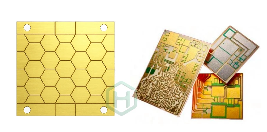
The continuous push for higher power density and higher switching frequencies in modern electronics—driven largely by SiC and GaN wide-bandgap (WBG) devices—demands substrates with superior thermal and electrical performance. In this context, advanced ceramic PCB technologies have become essential for managing heat and ensuring electrical stability in high-stress power environments.
The AlN ceramic circuit board, a high-performance member of the broader ceramic PCB family (also sold as aluminum nitride PCB), has emerged as a key platform in this space. It provides thermal management capabilities that conventional organic laminates and standard alumina (Al2O3) ceramics cannot match, while still supporting high-voltage isolation and stable RF behavior.
This article provides a technical perspective on AlN as a substrate material, comparing DBC and AMB copper bonding, explaining quantitative thermal validation, and outlining how packaging and turnkey assembly practices affect junction-to-case thermal resistance and long-term reliability—core considerations in modern PCB manufacturing workflows for WBG power and RF systems.
1. Thermal and electrical properties of AlN substrates
The value of an AlN ceramic circuit board starts with its intrinsic material properties. These directly influence power density, efficiency, and RF performance.
1.1 Thermal behavior and heat spreading
Key thermal properties of AlN relevant to power design:
Typical thermal conductivity:
Commercial AlN materials commonly range from roughly 140 to 230 W·m⁻¹·K⁻¹. Typical engineering grades used for AlN ceramic circuit boards are often quoted in the 170–220 W·m⁻¹·K⁻¹ range. The exact K value depends on purity, microstructure, and sintering/densification conditions.Maximum continuous operating temperature:
Significantly higher than FR4 and other organic laminates, supporting sustained operation in high-temperature environments.Coefficient of thermal expansion (CTE):
On the order of 4–5 ppm/K, which is closer to silicon than traditional PCB materials.
Note: CTE is temperature-dependent. AlN’s CTE is in the same order of magnitude as silicon (≈ 2.6–3 ppm/K) but typically somewhat higher, so multi-material stacks still require careful mechanical design and stress management.
Compared with alumina (Al2O3, thermal conductivity around 20–30 W·m⁻¹·K⁻¹), an AlN ceramic circuit board can move heat away from SiC or GaN junctions much faster. This reduces temperature gradients between the die and the baseplate or heatsink, and helps prevent thermal runaway in aggressively rated designs.
From a system perspective, this higher thermal conductivity allows:
- Higher allowable power dissipation for the same junction temperature limit
- Lower junction temperature at a given power level
- More compact module layouts without sacrificing lifetime
1.2 Electrical and RF characteristics
AlN is not only a thermal material; it is also an electrically robust and RF-friendly substrate:
Dielectric constant:
Relative permittivity εr ≈ 8.5–9.0 is typical for AlN used in circuit boards. Measured values depend on frequency, temperature, and test method (for example, 1–10 GHz characterization ranges are common in RF work).Low dielectric loss:
A low loss tangent is one of the key advantages. For many RF grades of AlN, tan δ is often ≤ 5 × 10⁻⁴ in the GHz range, although the exact number depends on frequency, temperature, and the measurement standard.High dielectric strength:
Suitable for kilovolt-level isolation barriers and high-voltage sections in power electronics.
For high-frequency power amplifiers, radar front-ends and 5G/6G equipment, these characteristics allow an AlN ceramic circuit board to support both high RF power and low-loss signal paths, with stable performance over temperature and time.
2. DBC vs AMB copper bonding on AlN
The performance of an AlN ceramic circuit board is not defined by the ceramic alone. The way copper is bonded to AlN is equally important, because it affects thermal resistance, mechanical robustness and fatigue life.
Two bonding methods dominate: Direct Bonded Copper (DBC) and Active Metal Brazing (AMB).
2.1 Direct Bonded Copper (DBC)
DBC bonds copper directly to AlN in a controlled atmosphere at high temperature.
Key technical points:
The process depends on maintaining appropriate temperature and oxygen levels so that a controlled interlayer forms between copper and AlN, ensuring adhesion and acceptable residual stress.
Power cycling can drive fatigue at the copper–ceramic interface, especially when voids or non-uniformities are present.
Void control:
Scanning Acoustic Microscopy (SAM) is commonly used to inspect the bond line. A realistic target is to keep total bond-line void area low—industry practice typically aims for ≤ 2% of the bonded area, with suppliers providing SAM maps and explicit acceptance criteria.
DBC is often the preferred solution for:
- Industrial power modules
- Solar inverters
- General-purpose high-power supplies
It offers a good balance between cost, thermal performance and reliability when cycling requirements are demanding but not extreme.
2.2 Active Metal Brazing (AMB)
AMB uses an active braze alloy to form a metallurgical bond between copper and AlN under high-vacuum conditions.
Technical aspects of AMB on AlN ceramic circuit boards:
An active element (typically titanium) in the braze alloy reacts with the AlN surface to form a strong interfacial layer (for example, Ti-based reaction products), improving bond strength and fatigue resistance.
AMB brazing usually runs at vacuum levels on the order of 10⁻³ to 10⁻⁵ mbar, combined with a tightly controlled temperature profile to avoid brittle phases and to ensure a uniform joint.
Peel or shear tests on coupons verify bond strength; results are commonly reported in N/mm (for peel) or MPa (for shear/tensile). AMB bonds generally show higher mechanical robustness and longer fatigue life than standard DBC joints when tested under comparable cycling conditions.
AMB is well suited for:
- EV traction inverters
- Heavy-duty industrial drives
- Applications where the module must survive many thousands of power cycles with large temperature swings
In practice, many designs start with DBC during early evaluation and qualification, and move to AMB when lifetime testing or field conditions show that fatigue margins are tight.

3. Thermal validation and lifetime prediction
Moving from material properties and process descriptions to real-world reliability requires quantitative measurement and analysis. This is where thermal characterization and lifetime modeling become essential.
3.1 Transient thermal characterization
Steady-state thermal resistance numbers alone are often not enough. For an AlN ceramic circuit board used in WBG power modules, engineers increasingly rely on transient thermal methods.
Using transient thermal analysis, it is possible to:
Build a structure function that conceptually separates the thermal path into sections (die, die attach, interface to AlN, AlN itself, baseplate, and so on).
Quantify how much each layer contributes to the overall junction-to-case thermal resistance.
Detect anomalies such as poor die attach or degraded bond lines, which may not be obvious from simple steady-state measurements.
Typical tools and methodologies include:
- Dedicated thermal transient testers capable of generating and analyzing structure functions
- Test procedures aligned with JEDEC or IEC standards for Rth measurement, where applicable
The result is a more accurate view of Rth(j-c) and better confidence that changes in process or design really improve (or at least do not worsen) the thermal path.
3.2 Power cycling and statistical lifetime models
Thermal measurements need to be connected to lifetime expectations. For an AlN ceramic circuit board in a power module, key mechanisms include:
- Fatigue of the copper–AlN interface (especially in DBC configurations)
- Fatigue of die attach layers (such as solder or sintered silver)
- Solder joint fatigue at module-level interconnects
Power cycling tests are used to stress these structures using realistic temperature swings and current profiles. The resulting failure data are commonly analyzed using Weibull statistics to determine:
- Characteristic life (the number of cycles at which a defined percentage of samples are expected to fail)
- Shape factor, which indicates how spread out the failure distribution is, and thus affects derating decisions
To make this data meaningful, it is important that:
- The applied temperature swing (ΔT), dwell times, and ramp rates in the cycling tests reflect the actual mission profile—for example, power-on/off durations, load patterns, and environmental conditions that the module will see in service.
This combination of realistic test conditions and appropriate statistical modeling allows engineers to predict field lifetime and justify choices such as DBC vs AMB, copper thickness, and die attach technology.
4. Managing Thermal Performance in High-Density Earbuds PCB Design
As earbuds become smaller yet more powerful, managing thermal buildup inside confined enclosures has become one of the most challenging aspects of earbuds PCB design. Poor heat control can lead to shorter battery life, degraded sound performance, and reduced user comfort — all of which directly impact product quality and brand reliability.
At HILPCB, our engineers implement a multi-layer thermal optimization strategy tailored for high-density rigid-flex PCB assemblies used in compact wearable electronics.
Key Thermal Management Techniques
- Pre-layout Thermal Simulation: Early-stage modeling identifies potential hot zones, allowing layout adjustments before production.
- Optimized Copper Plane Distribution: Strategic use of copper pours and ground segmentation enhances even heat spreading without compromising impedance control.
- High Thermal Conductivity Materials: Selective use of aluminum-backed laminates or high-thermal PCBs improves power efficiency and reduces local temperature rise.
- Localized Heat Dissipation: Focused design around charging ICs, amplifiers, and RF modules ensures stable performance under continuous load.
- Rigid-Flex Heat Path Integration: Embedded copper stiffeners or flex interconnects help transfer heat away from sensitive components, improving comfort and long-term reliability.
- Stack-Up and Material Optimization: Balancing dielectric thickness, copper weight, and thermal interface materials maintains RF integrity while controlling heat transfer.
5. Quality Systems and DFM for Complex AlN-Based Modules
AlN ceramic circuit boards are used in long-life, high-reliability products across automotive, industrial power, RF communications, aerospace and medical electronics. Consistent quality control and early DFM are essential to achieve predictable performance.
5.1 Quality Management and Traceability
High-reliability AlN manufacturing requires disciplined process control and full traceability, typically including:
- IATF 16949, AS9100, ISO 13485 or ISO 9001 depending on application requirements
- Lot-level tracking of AlN substrates, braze alloys, DBC/AMB furnace runs, metallization processes and final test results
- Stored inspection data such as SAM bond-line scans, peel/pull strength tests and electrical test logs
These controls ensure process stability and simplify root-cause analysis during long product lifecycles.
5.2 DFM for Thermo-Mechanical Reliability and Cost
Because AlN modules are costly to redesign, early DFM focuses on:
- Technology partitioning: Using AlN only where needed for thermal, dielectric or RF performance, and FR4/HDI/rigid-flex/MCPCB elsewhere to reduce cost
- Copper design: Selecting copper thickness and relief features (slots, rounded corners, trenches) to balance thermal spreading and interface stress
- Panelization and outline design: Optimizing panel layout and machining allowances to reduce material waste and improve assembly yield
A well-structured DFM approach minimizes risk and ensures the module meets its thermal and reliability targets.
AlN ceramic circuit boards enable compact, high-density WBG power and RF systems. Combined with controlled bonding, reliable die attach and disciplined DFM, they provide a robust foundation for long-life, high-performance electronics.