
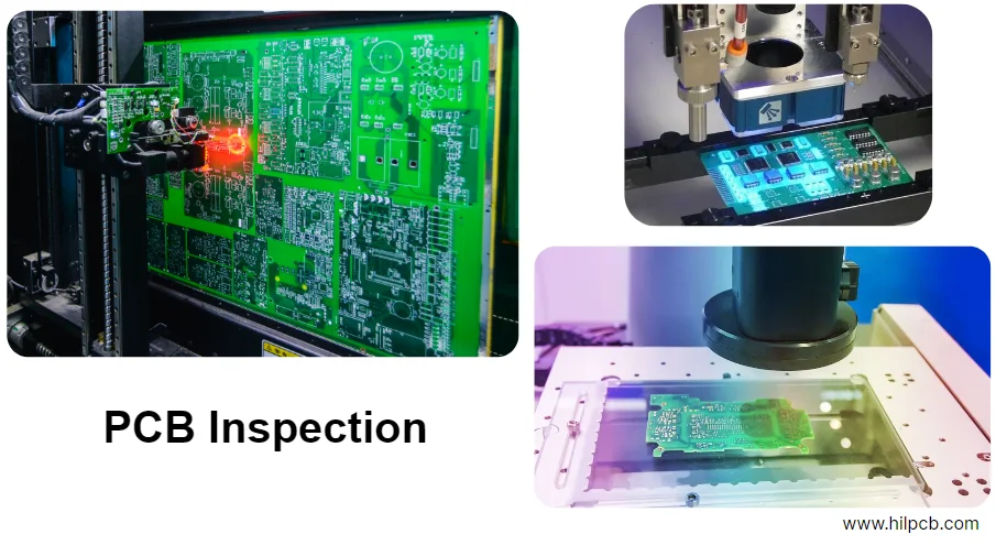
Executive summary: quality targets and business metrics
In today’s market for high-speed, high-reliability electronics, PCB manufacturing and assembly quality is the foundation that decides whether a product succeeds. Even tiny manufacturing deviations can cause field failures—leading to large economic loss and lasting brand damage. HILPCB’s operational-excellence philosophy is to build quality into every design stage through data-driven process control, advanced quality tools, and a deeply collaborative DFX (Design for Excellence) mechanism—rather than relying only on final test.
This white paper systematically explains HILPCB’s end-to-end quality management system. We cover every critical node from bare-board fabrication to SMT assembly, and then full test and traceability. The core focus is aoI spi best practices—showing how we use state-of-the-art equipment such as 3D SPI (solder paste inspection) and 3D AOI (automated optical inspection), together with SPC (statistical process control) and CPK (process capability) analysis, to achieve FPY > 99.5% and CPK > 1.67 on critical processes.
With hard data, mass-production cases, and a 35+ item DFM/DFT/DFR checklist, you’ll see how HILPCB turns a complex pcb manufacturing whitepaper into predictable, controllable, and traceable manufacturing excellence—helping you build a robust yield improvement roadmap and ultimately deliver higher reliability and market competitiveness.
PCB bare-board capability data
The bare PCB is the carrier for all electronic components; its manufacturing precision directly determines the final product’s electrical performance and reliability. With industry-leading process capability, strict parameter control, and continuous equipment upgrades, HILPCB ensures every PCB meets the most demanding design specifications. The table below summarizes our core capability metrics and representative mass-production cases for key processes.
| Process Step | Core Capability | Key Metric | Mass Production Case |
|---|---|---|---|
| Inner-layer circuitry | Minimum line width/spacing | 2.5/2.5 mil (0.0635mm) | 5G communication modules, high-speed server motherboards |
| Lamination | Max layer count / material types | 32 layers / Rogers, Megtron 6, FR4 High-Tg 180 | Aerospace control units, data-center switches |
| Mechanical drilling | Minimum hole / aspect ratio | 0.15mm / 16:1 | HDI boards, medical imaging equipment |
| Laser drilling | Minimum microvia diameter | 0.075mm (75μm) | Smartphone mainboards, wearables |
| Plating | Hole copper thickness / uniformity | Avg > 25μm / > 90% | Automotive ECUs, industrial power supplies |
| Solder mask | Solder-mask bridge accuracy | ≥ 3 mil (0.076mm) | BGA/CSP substrates, consumer electronics |
| Surface finish | Type / thickness control | ENIG, ENEPIG, OSP, HASL / Au: 1-3μ" | AI accelerator cards, IoT sensors |
Manufacturing strength: full-stack control from materials to finished goods
HILPCB’s capability is not only about pushing limits—it’s about deep understanding and control of the entire pcb fabrication process steps. We provide professional surface finish selection tips and a stackup documentation guide, helping you avoid manufacturing risks at the design source and achieve the best balance between cost and performance.
Quality tools: from statistical control to digital dashboards
Passive defect detection is no longer enough for modern manufacturing. HILPCB’s quality system is built on proactive prevention and continuous-improvement tools to keep processes stable and predictable.
SPC (Statistical Process Control) We apply SPC monitoring to key parameters such as plated copper thickness, etch width, and impedance. With X-bar & R control charts, we track process variation in real time. When trends approach or exceed control limits, the system triggers an alert and engineers intervene immediately—before nonconforming output becomes a batch issue.
CPK (Process Capability Index) CPK is a gold standard for whether a process can meet tolerance requirements. For all critical processes we target CPK ≥ 1.67 (6 Sigma level), meaning natural process variation is far smaller than the specification window—delivering high consistency and yield. For example, our drilling positional accuracy maintains CPK above 1.7, providing a solid foundation for high-density BGA placement.
MSA (Measurement System Analysis) Accurate decisions require reliable data. We regularly perform Gage R&R (repeatability and reproducibility) on measurement systems including AOI, SPI, flying-probe testers, and impedance testers—keeping measurement error below 10% of total tolerance and ensuring
cpk spcanalysis remains valid.8D (Eight Disciplines Problem Solving) When quality abnormalities occur, we launch a structured 8D process: build a cross-functional team, define the problem, implement containment, analyze root causes (fishbone, 5-Why), then define/validate permanent corrective actions and roll them out—ensuring issues are eliminated and do not recur.
Digital dashboard We provide customers with a secure online portal showing real-time production progress, in-process yield, SPC charts, and FPY data. This transparency lets customers understand project quality status as if they were on-site.
Quality tools: from statistical control to digital dashboards
SMT assembly is the defect-hotspot of PCBA manufacturing—over 60% of defects originate from solder paste printing. Therefore, building an inspection closed loop centered on SPI and AOI is the key to high yield. HILPCB’s aoI spi best practices is not just “buying advanced machines”—it’s a complete methodology.
Best practices for 3D SPI (Solder Paste Inspection)
- 100% inspection: We run 100% 3D inspection on solder paste for every pad, measuring volume, area, height, XY offset, and shape. This is far more reliable than traditional 2D inspection and effectively detects insufficiency/excess caused by stencil clogging, uneven squeegee pressure, and similar issues.
- Closed-loop feedback: Our SPI system communicates with the solder paste printer in real time. When SPI detects systematic print offsets (e.g., overall XY shift), it automatically sends correction commands to the printer, dynamically self-correcting print accuracy and killing defects at the source.
- Scientific tolerance settings: We avoid “one-size-fits-all” thresholds. Based on component types (e.g., 01005 capacitors vs. 0.8mm BGA) and pad sizes, we use historical data and IPC standards to set differentiated, more scientific SPI tolerances—significantly reducing False Calls.
Best practices for 3D AOI (Automated Optical Inspection)
- Multi-stage inspection strategy: Deploying 3D AOI after reflow is standard. For high-density or high-reliability projects, we add an AOI step before reflow to check misplacement, polarity, missing parts, and more—preventing defects from becoming difficult to fix after entering the expensive reflow oven.
- AI-enabled defect recognition: Traditional AOI depends on complex manual parameter tuning and tends to produce high false-call rates. HILPCB’s next-generation 3D AOI integrates AI deep-learning algorithms. Trained on massive defect image sets, the system identifies real defects more intelligently and accurately (cold joints, tombstoning, lead lift, etc.) while filtering pseudo-defects such as reflections and silkscreen interference.
- Central program library management: Inspection programs and standards for all components are stored on a central server. When a new project is imported, the system automatically calls the standard library—ensuring consistent inspection criteria across lines and shifts, and eliminating quality fluctuation caused by manual programming differences.
AXI (Automated X-ray Inspection) as a complement
For packages with hidden joints—BGA, QFN, LGA—AOI cannot help. In these cases, AXI becomes the last line of defense. Our 2.5D/3D AXI equipment clearly detects hidden defects such as BGA shorts/opens, Head-in-Pillow, and voiding. We provide a detailed x ray inspection checklist, and can deliver per-BGA X-ray reports on request.
Manufacturing strength: triple assurance with 3D SPI + 3D AOI + 3D AXI
HILPCB integrates 3D SPI, 3D AOI, and 3D AXI to build a full-process, 3D defect-detection network across SMT. Through data interconnection, this network captures over 99.9% of manufacturing defects—and uses analytics to guide process optimization, forming a continuous-improvement quality loop. This is a core competitive advantage behind our ultra-high straight-through yield.
Test coverage: ensure every function runs as intended
Perfect manufacturing does not guarantee perfect functionality. A comprehensive test strategy is the only way to validate that the product matches design intent. HILPCB works with customers to tailor optimal test plans based on complexity and application scenarios—maximizing test coverage and cost effectiveness.
| Test Method | Description | Coverage | Typical Defects Found |
|---|---|---|---|
| Flying Probe | No expensive fixture required; movable probes contact test points—ideal for prototypes and small runs. | Structural defects (shorts, opens) | Trace shorts/opens, unsoldered component leads. |
| ICT (In-Circuit Test) | Bed-of-nails fixture contacts all points at once; fast—ideal for volume production. | Structural defects; component-level parameters | Shorts, opens, wrong/missing parts, incorrect values (R/C), diode/transistor polarity errors. |
| FCT (Functional Test) | Simulates the final working environment and user operation to verify PCBA functions. | Functional defects | Power module failures, interface failures (USB/Ethernet), sensor reading errors, software logic issues. |
| Hipot (Dielectric Withstanding Voltage) | Applies high voltage to verify insulation strength and electrical spacing—key for safety compliance. | Insulation and safety defects | Insulation damage, insufficient creepage, component withstand-voltage issues. |
| Reliability Test | Uses ESS, HALT, etc. to simulate harsh environments. | Potential early-life failure defects | Cold joints, early component failures, PCB delamination, stress-induced micro-cracks. |
Improvement path: from test data to a yield improvement roadmap
Testing is not only about “sorting out bad boards”—it is also a valuable data source. HILPCB’s test system is deeply integrated with our data platform. We perform Pareto analysis on failure data to identify dominant defect modes, then feed results back into DFM/DFT. This data-driven feedback loop is the core of the yield improvement roadmap we build with customers—driving continuous improvements in yield and reliability across subsequent lots.
Traceability system: from data lake to visualization
When problems occur, quickly and precisely scoping impact is key to controlling loss. HILPCB builds an end-to-end traceability system—creating a unique “digital file” for every PCBA.
- Unit-level identity: Each PCB unit or panel is assigned a unique QR code or serial number when it enters production.
- Full-process data capture: From PCB incoming inspection, solder paste printing, pick-and-place, reflow, to AOI, ICT, and FCT, operators or equipment scan the code at every key station—binding people, equipment, time, material lots (e.g., a specific batch of ICs/resistors), process parameters (e.g., reflow temperature profile), and test results to the unique ID.
- Centralized data lake: All collected data streams into a secure centralized data lake in real time—forming a large, fine-grained manufacturing database.
- Visualization and bidirectional traceability:
- Forward trace: Enter a material lot number to instantly retrieve all PCBA serial numbers that used that lot.
- Reverse trace: Enter a PCBA serial number to query detailed production data via the portal—including which placement machine was used, the reflow profile at the time, and detailed ICT reports.
This traceability capability is not only a compliance requirement for demanding industries such as medical, automotive, and aerospace—it is also a powerful tool for root-cause analysis, continuous process optimization, and providing customers with maximum transparency and confidence.
DFM/DFT/DFR checklist: the foundation of collaborative design
The most successful projects start with tight collaboration between manufacturing and design. We encourage customers to work with our engineers early in the design phase. The checklist below is the core of our DFX review—helping you build a product that is manufacturable, testable, and highly reliable from the start.
| Category | Checklist Item | Rationale / Best Practice |
|---|---|---|
| DFM | Panelization | Prefer V-Cut to save space; use mouse-bites for boards with fragile components. Keep at least 5mm process rails around the panel. |
| DFM | Fiducial Mark | At least 3 per board; 3 on diagonal corners of the panel rails. 1mm mark with 2mm solder-mask clearance for accurate placement alignment. |
| DFM | Component spacing | Chip components > 0.5mm; spacing to BGA > 3mm for rework and AOI inspection. |
| DFM | Component orientation | Keep polarity part orientation (diodes, electrolytics) consistent to reduce placement errors. |
| DFM | Via design | Avoid Via-in-Pad unless using resin plug and planarization; otherwise solder wicking can cause insufficient solder and cold joints. |
| DFM | Pad design | Ensure footprints follow IPC-7351B—especially NSMD pads for BGA. |
| DFM | Solder mask dams | Dense-lead ICs (e.g., QFP) must have solder mask between pins (≥0.1mm) to prevent shorts during soldering. |
| DFM | Silkscreen | Do not print on pads or fiducials. Reference designators should be clear; polarity marks explicit. |
| DFM | Stack-up definition | Provide a complete stackup documentation guide (materials, thickness, copper weight, impedance) to avoid ambiguity. |
| DFM | Avoid Acid Traps | Avoid trace angles < 90° to prevent etchant entrapment and opens. |
| DFM | Teardrops | Add teardrops at pad-to-trace junctions to increase strength and reduce break risk from drill misregistration. |
| DFM | Copper-to-edge clearance | Keep copper at least 0.3mm from the routed edge (inner/outer layers) to prevent exposed copper and shorts. |
| DFT | Test Point size | ICT test points: diameter ≥ 0.8mm, pitch ≥ 1.9mm for stable probe contact. |
| DFT | Test Point distribution | Distribute evenly on both sides to avoid board bending from concentrated probe force. |
| DFT | Test Point cleanliness | No silkscreen/solder mask on test points; do not place under components. |
| DFT | Break out critical signals | Bring key signals (clock, reset, rails) to test points for debug convenience. |
| DFT | JTAG/SWD interface | For MCU/FPGA designs, reserve standard JTAG or SWD debug/programming interfaces. |
| DFT | Power isolation | Allow power domains to be isolated via jumpers or 0-ohm resistors for staged power-up and fault isolation. |
| DFT | Programmable devices | Ensure programmable ICs (Flash, EEPROM) have accessible programming interfaces. |
| DFT | Avoid test-point reuse | Avoid connecting test points directly to high-frequency or sensitive analog nets to prevent SI impact. |
| DFR | Thermal design | Add Thermal Vias under high-power devices and connect to large GND copper areas. |
| DFR | Component derating | Ensure components (especially capacitors, resistors, MOSFET) are properly derated for voltage/current/power. |
| DFR | Via protection | Fully cover Tented Vias with solder mask to prevent oxidation and accidental shorts. |
| DFR | High-voltage design | Follow safety creepage and clearance requirements. |
| DFR | Connector selection | Choose connectors with locating pegs or latches to improve mechanical strength and prevent vibration-related contact issues. |
| DFR | Material selection | Select board materials based on temperature/frequency (e.g., High-Tg FR-4) to prevent performance degradation at high temperature. |
| DFR | Decoupling capacitor placement | Place decoupling capacitors as close as possible to IC power pins for best filtering. |
| DFR | ESD protection | Add ESD protection near all external interfaces (USB, HDMI, antennas). |
| DFR | Conformal Coating | Reserve coating and keep-out areas (e.g., connectors) for PCBA that must operate in humid/dusty environments. |
| DFR | Vias under BGA pads | Vias under BGA pads must be plugged to prevent solder loss under BGA balls. |
| DFR | Crystal placement | Place crystals close to the MCU; avoid routing high-speed nets underneath to reduce interference. |
| DFR | Sensitive-signal protection | Use grounded shielding traces to surround differential pairs and sensitive analog nets for stronger SI. |
| DFR | Power-plane integrity | Keep PWR/GND planes continuous; avoid splits that disrupt current return paths. |
| DFR | Mechanical stress | Avoid placing fragile parts (e.g., ceramic capacitors) near edges, mounting holes, or connectors where stress is high. |
| DFR | Heatsink mounting | Reserve sufficient space and mounting holes for heatsinks and ensure a flat contact surface. |
HILPCB collaboration case and call to action
Case: a medical diagnostics manufacturer’s challenge and breakthrough
A leading medical-device startup hit a bottleneck while developing a new generation of portable ultrasound diagnostics. Its core mainboard was compact, integrating multiple 0.4mm-pitch BGA chips and thousands of 0201 components—placing extremely high demands on manufacturing and reliability. Their previous supplier delivered prototype-stage yields below 85% and could not provide detailed traceability data required for FDA submission.
HILPCB’s solution and results:
- Early deep collaboration: At project kickoff, our DFX engineers joined the design effort. Using our DFM/DFT checklist, we recommended adding 47 critical ICT test points and optimizing thermal via design in the BGA area—improving testability and thermal reliability at the source.
- Relentless process control: We used closed-loop 3D SPI to strictly control BGA solder paste volume, and 3D AXI to inspect every BGA at 100%, ensuring no Head-in-Pillow and voiding within limits. End-to-end
aoI spi best practicesensured highly consistent soldering quality. - Comprehensive test and traceability: We customized an ICT+FCT combined test plan, achieving over 98% fault coverage. We also provided unit-level traceability reports recording everything from material lots to key process parameters—fully meeting strict quality documentation requirements.
Outcome highlight: from uncertainty to full control
Through close collaboration with HILPCB, the customer increased PCBA FPY from 85% to 99.6% and shortened time-to-market by 6 weeks. More importantly, they gained fully transparent, traceable manufacturing data—providing a solid foundation for long-term reliability and regulatory compliance.
Your next high-reliability product should be built on the same strong quality foundation. Stop struggling with manufacturing uncertainty—let HILPCB be your trusted operational-excellence partner.
Ready to improve your product’s quality and reliability? Upload your Gerber and BOM files now to get a free professional DFM/DFT analysis report, and let our experts build a QA plan tailored to your needs.
Conclusion
This article explains aoI spi best practices across process capability, yield improvement, quality tools, test coverage, and traceability, and includes a DFM/DFT/DFR checklist to help teams build an effective collaboration mechanism—so you can systematically manage risk across design, materials, and test. By executing the checklist and process windows in this paper, and involving HILPCB’s DFM/DFA team early, you can accelerate prototype-to-volume delivery while maintaining quality and compliance.
For fabrication and assembly support, contact HILPCB via Turnkey Assembly or SMT Assembly for DFM/DFT guidance.