
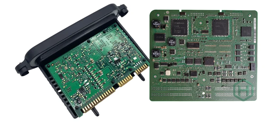
As an inverter control engineer, I know that in renewable energy, efficiency and power density are the eternal pursuit. From grid-tied PV systems to EV charging piles and energy storage systems (ESS), the three-phase inverter is the heart of energy conversion. At the heart of that heart, the performance of the power semiconductor device is decisive. In recent years, wide-bandgap semiconductors represented by silicon carbide (SiC) have been disrupting the dominance of traditional silicon (Si) IGBTs thanks to higher breakdown voltage, lower on-resistance, and ultra-fast switching. But to truly unlock SiC MOSFET performance, the key lies in its “brain” and “nervous system” — the gate driver circuit and the physical platform that carries it. This is where automotive-grade SiC MOSFET gate driver PCB becomes mission-critical: not just a connectivity board, but a platform that directly shapes inverter performance, reliability, and electromagnetic compatibility (EMC).
From the perspective of a system-level inverter engineer, this article breaks down the major challenges in designing and manufacturing a high-performance automotive-grade SiC MOSFET gate driver PCB—from gate-drive stability under ultra-high dv/dt, to high-voltage isolation under IEC/UL requirements, to suppressing power-loop parasitic inductance, controlling signal integrity, and finally achieving system-level thermal optimization and grid-compliance.
Unique challenges of SiC MOSFET gate driving: handling ultra-high dv/dt and common-mode noise
Switching from Si-IGBT to SiC MOSFET is far from a simple device swap. SiC MOSFETs switch roughly an order of magnitude faster than IGBTs, with dv/dt and di/dt reaching 50–100 V/ns and several A/ns. That extreme speed reduces switching loss—but it also makes PCB design for the gate-drive path dramatically harder.
1. Parasitic inductance: the root cause of gate ringing
During fast switching, any tiny parasitic inductance (L_parasitic) in the gate-drive loop forms an LC resonance with the SiC MOSFET input capacitance (C_iss). That inductance comes from PCB traces, component leads, and internal package bond wires. When the driver outputs a steep edge, the LC loop can ring at high frequency—“gate ringing”—which may cause:
- Voltage overshoot: gate voltage can exceed its maximum rating (often -10V to +25V), permanently damaging the device.
- False turn-on risk: a ringing valley can pull the gate below the Miller plateau during turn-off, causing unintended turn-on and shoot-through.
- Higher switching loss: ringing lengthens transition time and increases energy loss.
Following SiC MOSFET gate driver PCB best practices is the key. The core principle is to minimize gate-drive loop area. Practical actions include placing the gate driver IC as close as possible to the SiC MOSFET, using wide/short traces, and routing the drive and return paths (typically the source connection) in parallel and tightly coupled to leverage magnetic field cancellation. A well-planned SiC MOSFET gate driver PCB stackup—for example, placing the drive-signal layer adjacent to its return layer—can dramatically reduce loop inductance.
2. Common-mode transient immunity (CMTI): the isolation barrier stress test
In half-bridge or three-phase bridge topologies, when a SiC MOSFET (e.g., the low-side device) turns on, its source node can jump from 0 V to the DC bus voltage (V_DC) extremely fast, producing very high dv/dt. Through the isolation barrier parasitic capacitance of isolated gate drivers (optocouplers or digital isolators), that fast-changing potential couples into the primary-side logic control circuitry, creating common-mode current. If large enough, it can corrupt logic states and cause gate-drive errors.
Therefore, selecting an isolated gate driver with high CMTI (often >100 V/ns) is essential. Meanwhile, SiC MOSFET gate driver PCB design must support it: use an isolation “moat” or keep-out area beneath the isolation barrier to break the common-mode current path and improve immunity.
3. Miller effect and negative turn-off
High dv/dt also drives displacement current through the SiC MOSFET Miller capacitance (C_gd) during turn-off (i = C_gd * dv/dt). That current through the gate resistor can generate enough positive gate voltage to cause parasitic turn-on. To suppress Miller effect, SiC MOSFET gate driver PCB best practices typically include:
- Active Miller Clamp: during turn-off, the driver provides a low-impedance path to clamp the gate to source or to a negative rail.
- Negative gate turn-off voltage: providing -2 V to -5 V adds noise margin and keeps the device firmly off.
High-voltage isolation & safety: creepage/clearance design to meet IEC 62109
Renewable energy inverters connect to high-voltage DC (e.g., 800–1500 V PV strings) and the AC grid. Safety is the first priority. automotive-grade SiC MOSFET gate driver PCB must comply with IEC 62109 (PV inverter safety) or UL 1741, where the most fundamental physical requirements are Creepage and Clearance.
- Clearance: the shortest distance through air. It prevents air breakdown/arcing and depends on working voltage, altitude, and overvoltage category.
- Creepage: the shortest distance along the surface of an insulating material. It prevents tracking caused by pollution/humidity, and depends on working voltage, material group (CTI), and pollution degree.
Meeting these requirements in SiC MOSFET gate driver PCB design requires systematic planning:
- Functional partitioning: clearly separate primary (low-voltage control) and secondary (high-voltage drive) areas. Components, traces, and copper must respect the boundary.
- Physical isolation: add milling/slotting or cut-outs to increase creepage—often the most effective method. Slots must be wide enough to remain effective.
- Stackup considerations: an optimized SiC MOSFET gate driver PCB stackup matters; inner-layer HV and LV networks must also meet insulation requirements, determined by dielectric thickness and strength.
- Component selection: use safety-rated parts with sufficient pin pitch, such as isolated drivers, optocouplers, and transformers.
Achieving SiC MOSFET gate driver PCB compliance is not only “meeting the drawing”; it must also account for manufacturing tolerances. Working with an experienced manufacturer like HILPCB ensures isolation slots and spacing can be produced reliably. For example, when handling high current, Heavy Copper PCB not only carries current but also raises the bar for etching precision that affects creepage/clearance.
SiC MOSFET vs. Si-IGBT: key gate-drive design parameters
| Parameter | Si-IGBT | SiC MOSFET | PCB Design Impact |
|---|---|---|---|
| Typical switching speed (dv/dt) | 5-10 V/ns | 50-100 V/ns | Extremely sensitive to CMTI, EMI, and parasitic inductance. |
| Recommended gate-drive voltage | +15V / 0V or -8V | +18V to +20V / -2V to -5V | Requires asymmetric dual-rail supplies; higher demands on power design. |
| Threshold voltage (Vth) | ~5-6V (higher and stable) | ~2-4V (lower and temperature-sensitive) | Low noise margin; negative turn-off is close to mandatory. |
| Sensitivity to parasitic inductance | Medium | Very high | Gate-drive loop must be extremely compact and low-inductance. |
Power loop layout & DC-Link design: minimize loop inductance and voltage overshoot
Optimizing the gate-drive loop is only half the story. The parasitic inductance of the main power loop is another major root cause of voltage overshoot and EMI. This loop typically runs from the DC-Link capacitor positive terminal, through the high-side device, into the load, back through the low-side device, and returns to the DC-Link negative terminal.
When a SiC MOSFET turns off fast, the loop parasitic inductance (L_loop) generates a large induced voltage (V = L_loop * di/dt). That voltage stacks on top of the DC bus and appears directly across the MOSFET drain-source (V_ds). If V_ds exceeds avalanche breakdown, the device can fail instantly.
So SiC MOSFET gate driver PCB design must extend to the full power-module layout:
- Laminated bus / overlapping planes: the ideal low-inductance layout is a planar “sandwich”, where positive and negative power planes overlap over a large area, separated only by a thin dielectric. This uses magnetic-field cancellation to minimize loop inductance—often requiring multilayer boards and Heavy Copper PCB.
- Distributed DC-Link capacitors: besides bulk electrolytics, parallel multiple small, low-ESL film or ceramic capacitors close to each half-bridge. They provide the shortest path for high-frequency switching current and absorb transient energy.
- Snubber networks: in extreme cases, RC/RCD snubbers may still be needed to suppress spikes. Snubber design and placement are critical and must sit right at the MOSFET drain-source nodes.
Precision signal integrity: impedance control for automotive-grade SiC MOSFET gate driver PCB
When gate-drive edge rates reach the nanosecond range, PCB traces are no longer “wires”—they are transmission lines. If trace characteristic impedance is mismatched with driver output impedance and MOSFET input impedance, reflections occur, causing gate ringing and waveform distortion.
This is why SiC MOSFET gate driver PCB impedance control matters. The goal is to design transmission lines with a defined characteristic impedance (often 25–50Ω) to maximize power transfer and minimize reflections. Key enablers:
- Accurate calculation: impedance is set by trace width, distance to the reference plane (dielectric thickness), and dielectric constant (Dk). Use professional tools such as HILPCB’s Impedance Calculator to compute geometry early.
- Stable stackup: a clearly defined SiC MOSFET gate driver PCB stackup is the foundation. Ensure a continuous, unbroken reference plane (GND or VCC) below the trace; crossing splits creates impedance discontinuities.
- Manufacturing consistency: the PCB factory must tightly control laminate, dielectric thickness, and etching accuracy so final impedance matches the design. Tolerance control is critical for High-Speed PCB.
- Termination strategy: a small series resistor at the driver output (the gate resistor R_g) is a common source-termination method. It helps matching and actively damps LC resonance, but slightly slows switching—requiring a tradeoff between switching loss and ringing suppression.
Key design reminders
- Minimize the drive loop: The loop formed by driver IC, gate resistor, and MOSFET gate-source is the first optimization priority.
- Decouple power and drive loops: Avoid routing high-current power paths parallel to sensitive drive-signal paths to prevent noise coupling.
- Symmetric layout: For half-bridge or three-phase bridges, keep high/low-side drive and power paths as symmetric as possible for consistent switching dynamics.
- Ground strategy: Use star or multi-point grounding; connect control ground, drive ground, and power ground at defined single points to avoid ground-loop noise.
System-level thermal management & grid compliance: co-optimization from PCB to product
Even with high SiC efficiency, when handling kilowatts or even megawatts, heat is still significant. Higher power density means the heat is more concentrated. Effective thermal management is the lifeline of long-term inverter reliability.
Thermal strategies
Thermal design for automotive-grade SiC MOSFET gate driver PCB is a multi-physics problem:
- Enhance PCB heat spreading: add dense Thermal Vias under MOSFET pads to conduct heat into backside copper or directly into a heatsink. Metal Core PCB or IMS (insulated metal substrate) can be effective for surface-mount power devices.
- Optimize the heat path: minimize thermal resistance (R_th(j-a)) from junction to ambient via suitable packages (e.g., top-side cooling), TIM selection, and efficient heatsinks (air or liquid cooling).
- Temperature monitoring: place NTCs or sensors close to MOSFETs for real-time feedback to enable over-temperature protection and derating.
Grid compliance & EMI control
Renewable inverters must meet strict grid codes (e.g., IEEE 1547) and EMC standards. SiC fast switching generates wideband EMI. While LCL filters suppress current harmonics, a poor PCB layout can become a powerful EMI radiator, making the filter harder and more expensive.
EMI strategies to achieve SiC MOSFET gate driver PCB compliance include:
- Shielding and filtering: use the PCB ground plane as a shield, locally shield noise sources (e.g., switching nodes), and add proper common-mode and differential-mode filters at I/O and power entries.
- Control switching speed: within acceptable switching-loss increase, tuning gate resistor R_g can soften edges and reduce high-frequency EMI energy.
- System-level co-design: PCB layout, LCL filter design, and enclosure shielding must be co-optimized. Early simulation and strict EMC testing on prototypes are essential. HILPCB’s Prototype Assembly helps engineers iterate and validate quickly, accelerating time-to-market and certification.
Conclusion
The transition from Si to SiC is a major leap for renewable energy inverters, enabling unprecedented efficiency and power density. But success hinges on a seemingly “basic” yet critical element: automotive-grade SiC MOSFET gate driver PCB. It is no longer just a carrier for components—it is a complex system platform integrating high-voltage isolation, precision driving, power delivery, signal integrity, and thermal management.
Engineers must apply a holistic mindset and embed SiC MOSFET gate driver PCB best practices from concept through manufacturing. Whether it is controlling parasitics via SiC MOSFET gate driver PCB stackup, or ensuring waveform quality via SiC MOSFET gate driver PCB impedance control, every detail impacts inverter performance and reliability. Partnering with a PCB supplier with advanced manufacturing capability and deep engineering experience (such as HILPCB) is key to executing these complex designs precisely and meeting stringent SiC MOSFET gate driver PCB compliance requirements. A truly excellent automotive-grade SiC MOSFET gate driver PCB is the solid foundation for mastering high-voltage/high-current challenges, unlocking SiC potential, and powering a greener energy future.
Common Questions
Why is an automotive-grade SiC MOSFET gate driver PCB harder than a conventional inverter control board?
Because SiC switching pushes dv/dt, EMI, isolation stress, thermal density, and parasitic sensitivity much higher. The PCB is not just a carrier; it becomes part of the electrical and thermal design itself.
Why must isolation, EMI control, and layout be designed together on a SiC gate driver PCB?
Because creepage, return-current behavior, switching-node coupling, and common-mode noise all interact. Solving one area in isolation often creates a new problem in safety margin, waveform quality, or EMC performance.
Why do thermal management and impedance control matter so much in these designs?
Because unstable temperature and poor interconnect control can distort drive waveforms, increase overshoot, stress devices, and reduce long-term reliability. Performance depends on both heat removal and clean signal behavior.
Why does an experienced PCB manufacturing partner matter for automotive-grade SiC projects?
Because these boards demand tight process control in stackup, isolation geometry, copper balance, drilling, and inspection. A capable supplier helps convert simulation intent into hardware that can actually pass validation and compliance testing.