
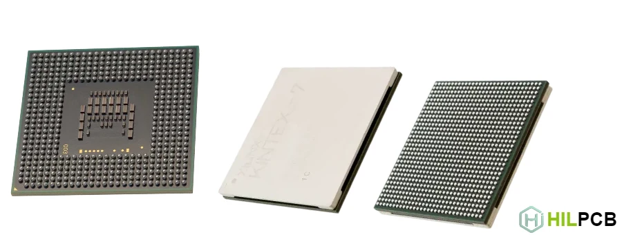
Ball Grid Array (BGA) packages have become the dominant interconnection technology for high-performance integrated circuits. BGA assembly enables higher I/O density, improved electrical performance, and better thermal dissipation compared to traditional leaded packages. However, successful BGA assembly demands precise process control, specialized equipment, and rigorous inspection protocols that distinguish capable manufacturers from those unprepared for advanced packaging.
HILPCB provides professional BGA assembly services with the equipment, expertise, and quality systems required for reliable ball grid array manufacturing across prototype through high-volume production.
Menu Navigation
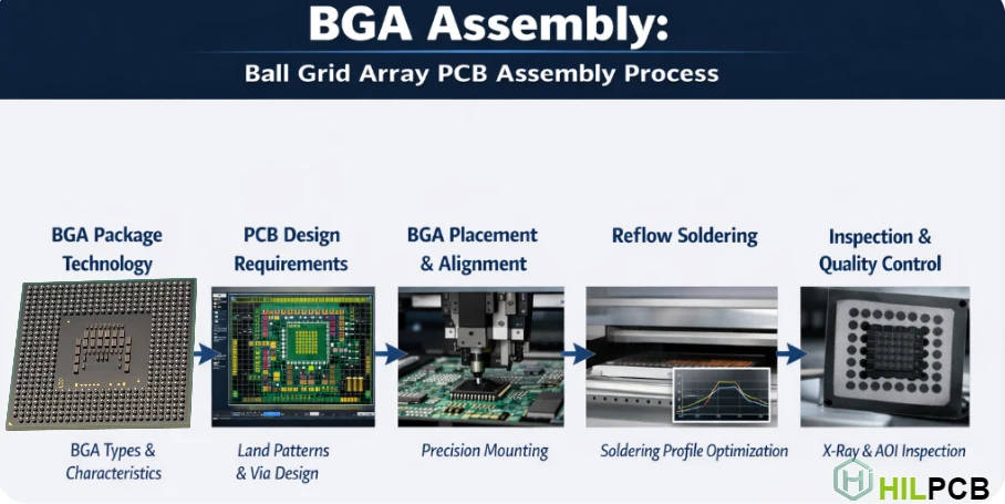
- Understanding BGA Package Technology
- PCB Design Requirements for BGA Assembly
- BGA Placement and Alignment Process
- Reflow Soldering Profile Optimization
- Quality Control and Inspection Methods
- Common BGA Assembly Challenges
- HILPCB BGA Assembly Capabilities
Understanding BGA Package Technology
BGA packages use an array of solder balls on the package underside to create electrical and mechanical connections to the PCB. This architecture offers significant advantages over peripheral-leaded packages, but introduces unique assembly considerations.
Package selection affects assembly complexity, reliability, and cost. Understanding the differences between BGA variants helps designers make informed decisions and enables manufacturers to optimize processes accordingly.
BGA Package Types
- Plastic BGA (PBGA): Standard package with laminate substrate and overmolded plastic body; most common for consumer and industrial applications; ball pitches typically 1.0mm to 1.27mm.
- Ceramic BGA (CBGA): Ceramic substrate provides superior thermal performance and hermetic sealing capability; used in high-reliability applications; higher cost but better CTE matching to ceramic PCBs.
- Chip Scale Package (CSP): Package area less than 1.2x die size; ball pitches 0.5mm and below; requires fine pitch BGA assembly techniques and HDI PCB substrates.
- Micro BGA (μBGA): Ultra-fine pitch packages with 0.3mm to 0.4mm ball spacing; used in mobile devices and dense computing applications; demands highest assembly precision.
- Package-on-Package (PoP): Stacked BGA configuration with memory mounted on logic device; common in smartphones; requires specialized stacking equipment and dual reflow capability.
- Flip Chip BGA (FCBGA): Die attached face-down with direct bump connections; provides best electrical performance; used in high-frequency and high-power applications.
Solder Ball Characteristics
Solder ball composition, size, and standoff height directly affect assembly process parameters and long-term reliability. Lead-free transitions have shifted most applications to SAC (tin-silver-copper) alloys.
PCB Design Requirements for BGA Assembly
Successful BGA assembly begins with proper PCB design. Land pattern geometry, via structures, and routing strategies significantly influence both manufacturing yield and field reliability.
Design decisions made early in the development cycle determine assembly feasibility and affect inspection capabilities. Collaboration between design and manufacturing teams prevents costly redesigns.
Land Pattern Design
- Non-Solder Mask Defined (NSMD) Pads: Preferred for most applications; copper pad smaller than solder mask opening; provides stronger solder joint with fillet formation on pad sidewalls; better inspection visibility.
- Solder Mask Defined (SMD) Pads: Solder mask overlaps copper pad edge; used when trace routing requires larger copper features; less preferred due to reduced joint strength.
- Pad Size Optimization: Land diameter typically 80-90% of ball diameter for NSMD; oversized pads increase bridging risk; undersized pads reduce joint strength and self-alignment capability.
- Solder Mask Registration: Minimum 75μm clearance between pad edge and solder mask for NSMD; tighter tolerances require advanced imaging and registration capability.
- Surface Finish Selection: ENIG provides flat, solderable surface ideal for BGA; OSP acceptable for single-reflow applications; immersion silver and tin offer cost alternatives with handling considerations.
Via-in-Pad Considerations
Via placement under BGA pads presents assembly challenges but often proves necessary for signal escape in dense arrays. Proper via treatment prevents defects while enabling routing density.
- Filled and Capped Vias: Conductive or non-conductive fill with copper plating cap; provides flat pad surface for reliable solder joint; required for via-in-pad designs.
- Plugged Vias: Epoxy fill without planarization; acceptable for some applications but may cause pad coplanarity issues affecting solder paste deposition.
- Open Vias: Never acceptable under BGA pads; solder wicks into via creating voiding and insufficient joint volume; common cause of assembly failures.
- Via Size Limits: Smaller vias easier to fill reliably; 0.3mm finished hole diameter or smaller recommended for via-in-pad; larger vias require special fill processes.
Routing and Escape Strategies
Signal escape from dense BGA arrays requires careful planning balancing electrical performance, manufacturing capability, and layer count economics.
BGA Placement and Alignment Process
BGA placement requires precision equipment capable of accurate alignment despite hidden solder connections. Modern pick-and-place machines use vision systems that reference package fiducials and pad patterns to achieve required accuracy.
Placement accuracy directly affects self-alignment during reflow. While BGA packages exhibit significant self-centering behavior, excessive initial offset can result in bridging, open connections, or shifted components that fail inspection.
Placement Equipment Requirements
- Vision System Capability: Upward and downward looking cameras for simultaneous package and board alignment; minimum resolution for ball-level inspection on fine pitch devices.
- Placement Accuracy: Machine capability index (Cpk) matched to ball pitch; 0.5mm pitch requires ±50μm accuracy at 3σ; finer pitches demand proportionally tighter control.
- Component Handling: Proper nozzle selection and vacuum levels prevent package damage; large BGAs require adequate support during transport; moisture-sensitive handling protocols.
- Placement Force Control: Excessive force damages solder balls; insufficient force causes placement instability; programmable force profiles accommodate different package types.
- Fiducial Recognition: Global and local fiducial systems compensate for board stretch and registration; component-level fiducials critical for fine pitch placement.
- Height Sensing: Z-axis position control ensures consistent ball contact without crushing; accounts for board warpage and component thickness variation.
Pre-Placement Preparation
Component and board preparation significantly affects placement success and solder joint quality. Moisture control proves particularly critical for BGA packages.
- Moisture Sensitivity Level (MSL) Management: BGA packages absorb moisture during storage; rapid heating during reflow causes "popcorning" delamination; baking protocols restore dry condition before assembly.
- Component Inspection: Incoming inspection verifies ball coplanarity, contamination, and damage; rejected components removed before placement; traceability maintained.
- Board Preparation: PCB cleaning removes handling contamination; plasma treatment improves solder paste adhesion on difficult surfaces; proper support prevents warpage during printing.
Reflow Soldering Profile Optimization
Reflow profile development for BGA assembly balances multiple constraints including solder paste activation, flux performance, thermal uniformity, and component thermal limits. Profile optimization directly affects BGA soldering defect rates and long-term reliability.
BGA packages present unique thermal challenges due to their mass and hidden connections. The package body shields solder joints from direct heating, requiring longer soak times and potentially higher peak temperatures than exposed surface mount joints.
Reflow Profile Zones
- Preheat Zone: Gradual temperature rise (1-3°C/second) evaporates solder paste volatiles; prevents solder spattering; reduces thermal shock to components; typical endpoint 150-200°C.
- Soak Zone: Temperature stabilization allows flux activation and thermal equalization across the board; critical for BGA due to package thermal mass; typically 60-120 seconds duration.
- Reflow Zone: Rapid heating to peak temperature melts solder; SAC alloys require 235-250°C peak depending on paste formulation; time above liquidus (TAL) typically 40-90 seconds.
- Cooling Zone: Controlled cooling rate (2-4°C/second) develops proper grain structure; excessive cooling rates stress joints; insufficient rates allow intermetallic growth.
Profile Development Methodology
- Thermocouple Placement: Direct attachment to BGA body and PCB surface; measurement at coldest and hottest board locations; minimum 5-point profiling for complex assemblies.
- Thermal Mass Considerations: Large BGAs require extended soak times; multiple large packages may create thermal shadows; board support affects heat transfer.
- Atmosphere Selection: Nitrogen atmosphere reduces oxidation enabling lower residue fluxes; particularly beneficial for lead-free processes with narrow process windows.
- Profile Documentation: Validated profiles documented with tolerance bands; regular verification ensures process stability; adjustments tracked and qualified.
Quality Control and Inspection Methods
BGA inspection presents fundamental challenges because solder joints hide beneath the package body. Visual inspection cannot assess joint quality, requiring specialized techniques to verify assembly integrity.
Inspection strategy combines multiple methods to provide comprehensive defect coverage while maintaining production throughput. Each technique offers specific capabilities and limitations that informed manufacturers use appropriately.
Automated Optical Inspection (AOI)
- Placement Verification: Confirms component presence, position, and orientation before reflow; identifies gross misalignment that may cause bridging.
- Post-Reflow Limitations: Cannot see solder joints under BGA; limited to peripheral ball visibility on some packages; detects lifted or missing components.
- Solder Paste Inspection (SPI): Pre-placement verification of paste volume and registration; critical for consistent solder joint formation; 3D SPI provides volume measurement.
X-Ray Inspection
BGA X-ray inspection provides the only non-destructive method to visualize solder joints beneath BGA packages. Modern X-ray systems offer 2D and 3D imaging capabilities essential for BGA quality verification.
- 2D X-Ray Imaging: Transmission images show ball shape, voiding, and bridging; quick inspection suitable for sampling; limited depth information may obscure defects.
- 3D Computed Tomography (CT): Reconstructed cross-sections provide complete joint visualization; identifies defects obscured in 2D views; slower throughput but superior detection.
- Automated X-Ray Inspection (AXI): Programmed inspection with automatic defect detection; enables 100% inspection at production rates; algorithm optimization critical for accuracy.
- Void Measurement: X-ray quantifies void percentage in solder joints; IPC standards define acceptable limits; excessive voiding indicates process issues requiring correction.
Functional and Reliability Testing
Inspection detects visible defects but cannot guarantee electrical functionality or long-term reliability. Test strategies complement inspection to provide complete quality assurance.
Common BGA Assembly Challenges
BGA assembly introduces failure modes not present with leaded packages. Understanding common defects enables prevention through process control and rapid correction when issues occur.
Defect analysis requires correlating inspection findings with process parameters and design characteristics. Systematic problem-solving approaches identify root causes rather than addressing symptoms.
Typical Defect Categories
- Solder Bridging: Adjacent balls connected by excess solder; caused by excessive paste volume, misalignment, or pad design issues; detected by X-ray showing merged balls.
- Head-in-Pillow (HiP): Partial connection where paste and ball partially melt but don't fully coalesce; caused by package warpage during reflow; appears acceptable in X-ray but fails electrically.
- Open Connections: Insufficient solder or non-wetting prevents joint formation; caused by contamination, oxidation, or inadequate paste volume; electrical test detects failures.
- Voiding: Gas bubbles trapped in solder joint reduce strength and thermal conductivity; caused by flux outgassing, paste chemistry, or pad contamination; X-ray quantifies severity.
- Ball Fracture: Cracked solder balls from mechanical stress; caused by board flexure, thermal cycling, or drop impact; may not fail immediately but progresses over time.
- Component Warpage: Package deformation during reflow creates non-coplanar ball array; causes opens at corners and center depending on warpage direction; package-specific phenomenon.
Understanding these defects and their causes guides prevention strategies. For detailed analysis of specific failure modes and corrective actions, see our comprehensive guide to BGA soldering defects.
Process Control Strategies
Preventing defects requires controlling input variables, monitoring process parameters, and implementing feedback systems that detect drift before defects occur.
HILPCB BGA Assembly Capabilities
HILPCB provides comprehensive BGA assembly services with the equipment, processes, and quality systems required for reliable production across package types and volumes.
Why Choose HILPCB for BGA Assembly
Advanced Placement Equipment
Our SMT lines feature high-accuracy placement machines capable of BGA assembly down to 0.3mm pitch. Vision systems provide precise alignment for both standard and fine pitch BGA assembly, with placement accuracy meeting IPC Class 3 requirements.
Comprehensive X-Ray Inspection
Every BGA assembly receives X-ray inspection with our advanced imaging systems. 2D and 3D inspection capabilities detect hidden defects including voids, bridges, and head-in-pillow conditions that visual inspection cannot identify.
Optimized Reflow Processing
Nitrogen reflow with precise profile control ensures consistent solder joint formation. Our thermal profiling capabilities accommodate complex assemblies with multiple BGA packages and varying thermal masses.
Rework and Repair Capability
When defects occur, our BGA rework stations enable professional repair without board damage. Controlled heating profiles and precision alignment preserve component and PCB integrity during rework operations.
Reballing Services
Components requiring solder ball replacement benefit from our BGA reballing capabilities. Whether salvaging components from failed assemblies or reconditioning moisture-damaged packages, we restore components to specification.
Production Flexibility
- Prototype assembly for design verification with full inspection
- Small batch production with sampling-based quality protocols
- Volume manufacturing with statistical process control
Design for Manufacturing Support
Our engineering team reviews BGA designs before production, identifying potential assembly challenges and recommending optimizations. DFM feedback prevents yield issues and improves first-pass success rates.
Submit your BGA assembly project for manufacturing review and quotation. Our team provides specific recommendations for your design complexity and volume requirements.
Common Questions
What makes BGA assembly different from standard SMT assembly?
BGA packages use hidden solder balls under the component, so placement, stencil, and reflow control must be tighter than for leaded or visibly jointed SMT parts.
Why is placement accuracy important in BGA assembly?
Small alignment errors can reduce solder joint quality or create opens and bridges because the electrical connections are concentrated under the package.
How are BGA solder joints inspected?
Manufacturers typically use X-ray inspection, supplemented by AOI, rework evaluation, and process monitoring because the joints cannot be fully seen from the outside.
Can the same BGA process support prototypes and volume production?
Yes. A capable assembler can support both when it has stable profiles, repeatable inspection criteria, and documented control from first articles through production ramps.