

A BGA joint forms out of sight. The paste is printed, the package is placed on top of it, and the ball, paste and pad have to melt and merge while the package and board both bend with temperature. Every BGA defect starts with one of three failures in that sequence: wrong solder volume at a site, lost contact between ball and paste while they are molten, or gas trapped as the solder freezes.
Because the joint is hidden, an electrical test result or an X-ray image only covers part of it. Sorting defects by mechanism, and knowing the contact and solder-volume margins behind each one, tells you which inspection can answer the question and which corrective action addresses the cause. For the full assembly flow, see BGA assembly. For component removal and replacement, see BGA rework.
1. Classify by electrical behavior, then by mechanism
| Class | Electrical behavior | Typical mechanisms | Detection difficulty |
|---|---|---|---|
| Hard short (bridge) | Unwanted connection between balls | Excess paste, placement offset, package edge compression | Easy if nets differ; same-net bridges escape electrical test |
| Hard open | No connection | Lost contact from warpage, missing paste, non-wetting pad | Easy by test; locating the cause is harder |
| Resistive joint | Connected, abnormally high resistance | Partial coalescence, cracked interface, heavy interfacial voiding | Passes simple continuity; needs 4-wire or margin testing |
| Intermittent | State changes with temperature, flex or time | Head-in-pillow, pad cratering, micro-crack | Hardest; often reads "no fault found" at room temperature |
| Latent reliability | Passes all tests at build | Voids at interface, thin or missing intermetallic, stress risers | Found only by physical analysis or after field stress |
Record which class you have before picking a remedy. A hard open at three corner balls and an intermittent at one interior ball call for different investigations, even if both are logged as "BGA open".
2. Preserve evidence before rework
Rework heats the joint again and destroys the original interface. Before anyone touches the board:
- Map coordinates. Package drawings usually show the ball side (bottom view), while board maps are top view, so the two are mirror images. Convert the failing net to a ball ID (such as A1 or P14) and to a board coordinate, and check the conversion with a second person.
- Pull the process record. Retain SPI data for those pads, the placement log, the reflow profile and thermocouple positions, the paste lot, the component date code and MSL floor life.
- Choose a comparison unit. Pick a board from the same lot and line that passed. An unrelated passing board is weak evidence.
- Agree disposition. Decide which units are kept for analysis and which are reworked to recover hardware. A successful repair does not identify the cause.
3. Bridges: find the stage where the solder first connected
A BGA bridge connects two adjacent balls. If the balls are on different nets, it is a hard short. If they share a net (for example two GND balls), electrical test passes and only X-ray finds it. It is still a workmanship defect unless the land pattern was deliberately designed as a shared pad.
Bridges form at one of three stages, and the retained records can show which one:
| Stage | Evidence | Mechanism | Action to evaluate |
|---|---|---|---|
| SPI shows high volume, offset or a connected deposit at the bridged pads | Stencil misregistration, gasketing failure, damaged aperture, underside contamination | Stencil wipe interval, aperture condition, alignment; check that pad-to-pad mask web is present | |
| Placement | SPI normal; pre-reflow image shows offset or deposits squashed together | Excess Z overtravel, placement offset, deformed balls | Placement force and Z height, vision alignment, incoming ball coplanarity |
| Reflow | Print and placement normal; bridge only after reflow, often at package edge | Package edge pressing down during reflow (the reverse of the corner lift in Section 4), paste slump, excessive time above liquidus | Package warpage data at temperature, profile, paste slump behavior |
Reducing the aperture is often the first reaction and often the wrong one. A smaller deposit at the edge of a package that dips down during reflow is the same deposit that starves the corners when it lifts. Check the contact budget in Section 4 before cutting volume. HILPCB's SMT assembly route runs 3D SPI on BGA builds when specified, so print-stage bridges show up before placement. For visible fine-pitch bridges on leaded parts, see SMT solder bridge prevention.
4. Opens and warpage: the contact budget
An open is a lost contact between ball and paste that never recovered. Warpage is the most common reason it is lost, because both the package and the board change shape on the way to peak temperature.
Shape and sign. Describe warpage by geometry: corners up (concave, often called "smile") or center up (convex, "frown"). Naming conventions depend on which side you view from, so state the sign convention used in the data, such as the convention in JEDEC JESD22-B112 shadow-moiré measurement. Many packages change shape between room temperature and peak reflow, so the room-temperature shape tells you little about contact at liquidus. TI's PoP assembly guidelines (SWPA156) describe temperature-dependent package warpage as a cause of opens.
Corner contact budget. To first order, a corner ball keeps contact if the paste height exceeds the combined local separation of package and board at that site. The board's contribution follows from IPC bow-and-twist: a 0.75% bow on a 200 mm board is 1.5 mm across the board, but under a 35 mm package (uniform curvature, sagitta ∝ L²) only:
| Case (0.50 mm ball) | Paste height | Package corner lift | Board at site | Margin |
|---|---|---|---|---|
| A: moderate package, flat board | 125 µm | 50 µm | 0 | +75 µm |
| B: package and board bending in opposite directions | 125 µm | 80 µm | +45.9 µm | −0.9 µm |
| C: board bending the same way as the package | 125 µm | 80 µm | −45.9 µm | +90.9 µm |
| D: as B, stencil reduced to 100 µm | 100 µm | 80 µm | +45.9 µm | −25.9 µm |
This budget ignores ball collapse and paste slump, but it shows the sensitivities (calculation). The same board bow can either cancel or add to package warpage at a given corner. Case D shows why a stencil thinned to cure a bridge (Section 3) can turn a marginal corner into an open. Corrective actions follow from the budget: package warpage specification at temperature, board copper balance and symmetric stackup, support pins or a carrier under large boards, and a profile that lowers the temperature difference across the package. HILPCB's multilayer PCB route controls warpage typically below 0.75%. For a board that must stay flatter under a large BGA, give the requirement for that area separately.
Non-wetting opens. Contact can be maintained while the pad still does not wet. Typical causes are an oxidized or contaminated surface finish, a black-pad condition on ENIG, or paste flux used up before the solder melts. The sign is a ball that has collapsed and has formed an intermetallic on the package side only. Investigate pad finish lots and storage, and compare with known-good boards before changing the profile.
5. Head-in-pillow: contact is not coalescence
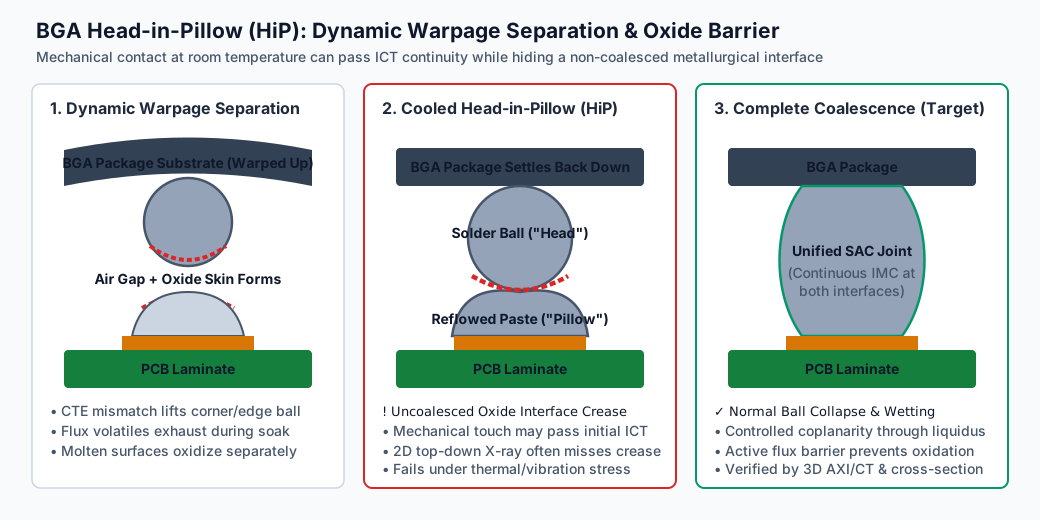
In a head-in-pillow (HiP) joint, both the ball (the "head") and the reflowed paste (the "pillow") have melted but did not merge. The ball rests in a dent in the paste with an oxide-lined crease between them. Mario Scalzo's HiP technical paper (hosted by IPC) describes ball and paste that both reflow but fail to coalesce, with warpage and wetting as drivers. AIM's head-in-pillow paper notes that such joints can initially conduct. The basic sequence:
- Separation. During the ramp toward liquidus, the package corner lifts (Section 4) and the ball moves away from the paste.
- Oxidation. Both surfaces are exposed. Paste flux is used up during a long soak, and the ball surface oxidizes. Stored components can already carry a thicker oxide.
- Return without merging. As the package flattens, near the peak or while cooling, the ball comes back down onto paste that has a skin of oxide. Neither surface has enough flux left to break the oxide, and the joint freezes with mechanical contact but no metallurgical bond across the crease.
That sequence explains the field behavior. The joint can pass room-temperature continuity and ICT because the ball physically touches the paste. It then opens with heat, vibration or board flex. Factors that lengthen the separation window or weaken flux make HiP more likely: a long soak, high temperature difference across the package, aged components, a low-activity paste, and thin deposits that leave little margin for contact.
Actions, matched to the step they act on:
| Step | Action to evaluate | Tradeoff to check |
|---|---|---|
| Separation | Package warpage spec at temperature; board support; lower ΔT across the package | Support tooling must not touch bottom-side parts |
| Separation | Keep paste height margin (do not thin the stencil blindly) | Bridge risk at package edge |
| Oxidation | Shorter soak or ramp-to-spike profile; HiP-resistant paste with longer flux activity | Voiding and flux outgassing, other components' profile windows |
| Oxidation | Nitrogen reflow atmosphere | Cost; some fluxes behave differently in N₂ |
| Oxidation | Component storage and floor-life control | Moisture-sensitivity bake can also age the ball surface |
6. What each inspection method can establish
| Method | What it can show | What it cannot clear |
|---|---|---|
| Electrical test (ICT, continuity) | Connection under the test condition at that moment | HiP, resistive and intermittent joints that touch at room temperature |
| Boundary scan | Pin-level connectivity where the device supports it | Joint quality; same-net bridges |
| 2D X-ray, top-down | Bridges, missing balls, gross voids, ball size and shape | HiP crease and pad cratering, which lie in the plane hidden by the ball's own projection |
| Oblique-angle X-ray, laminography, CT | Joint profile from other angles; the HiP shape (ball resting in a dent of paste) can sometimes be seen | Results depend on resolution, the board's other layers and the setup. A clean image is evidence for those joints under that setup, not a general clearance |
| Dye-and-pry | Which interfaces had already separated (dyed fracture surfaces) across the whole array | Destroys the sample; the pry can create new fractures that must be told apart from dyed ones |
| Cross-section (microsection) | Interface, intermetallic, cracks and voids in the polished plane | Only that plane at the selected joints; preparation can smear or damage features |
Two consequences matter in practice. First, a top-down 2D X-ray that reports "no defect found" on a net with a confirmed open does not end the investigation. Second, a cross-section that shows a sound joint may simply have missed the crack, or the open may be in the board: the via knee, the capture pad or the trace. Before the only failed unit is consumed, decide the order of tests: non-destructive methods first, then dye-and-pry or section, because a pried joint cannot also be sectioned. Agree the investigation question and sample disposition with the analyst. HILPCB's assembly routes apply selected X-ray to agreed hidden-joint risks and retain SPI/AOI/X-ray records and reflow profiles with the build.
7. Voiding and via-in-pad
Voids are gas pockets that were still in the joint when the solder froze. Indium's voiding note traces most of them to flux volatiles that could not escape while the solder was molten. Board-side sources add to that: residues on the pad, moisture, and above all open or poorly capped vias in the pad.
Via-in-pad wicking. An open via in a BGA pad is a capillary that pulls molten solder away from the joint. With a 1.0 mm pitch BGA, 0.50 mm balls and a 0.45 mm × 125 µm aperture (paste about 50% metal by volume):
| Volume | mm³ |
|---|---|
| Solder ball, 0.50 mm | 0.0654 |
| Metal from printed paste | 0.0099 |
| Open through-via, 0.20 mm finished × 1.6 mm | 0.0503 |
| Unfilled microvia, 0.10 mm × 75 µm | 0.0006 |
An open through-via (calculation) can hold five times the paste metal and three-quarters of the ball, so wicking can leave a starved or open joint. A microvia holds little solder, but it traps air and flux that bubble into the joint as interface voids. The board fix is via-in-pad plated over (VIPPO): resin or copper fill with a planarized copper cap. Specify the cap dimple limit with the fabricator. HILPCB's HDI PCB route builds VIPPO for fine-pitch BGA pads.
Report void data in a comparable form. A 2D X-ray void percentage is the void area projected through the ball. A void whose diameter is 30% of the ball diameter is only 9% of the area. Whether a report quotes diameter or area, the largest void or the total, and whether one image or several stacked planes were used, changes the number. Location matters more than total: a planar void at the pad interface carries load and heat through a reduced area, while a mid-ball void of the same size usually matters less. The acceptance criterion comes from the contract, typically IPC-A-610 at the agreed class plus any customer limit. IPC-7095 gives design and process guidance for BGAs. State the document, revision and measurement convention with every void result, rather than quoting a universal percentage limit.
Process levers. Paste chemistry with lower volatile content, a profile with a soak or slower ramp that lets volatiles escape before liquidus, and vacuum reflow for thermal pads and power devices with high void sensitivity. Each lever interacts with HiP (Section 5), so check the HiP risk after any profile change.
8. Worked investigation: intermittent open at U3
Each observation below changes the next step. The diagnostic worksheet lists other branches.
Symptom. A board passes ICT at room temperature. Functional test fails intermittently after warm-up, tracked to a path through U3 (a 35 mm, 1.0 mm pitch BGA).
| Step | Observation | What it supports | What remains open | Next action |
|---|---|---|---|---|
| 1. Map | Failing path resolves to balls A1, A2, B1 at one corner after bottom-to-top view conversion | Corner location fits a warpage-driven contact loss | Board-side failure at the same corner | Freeze the unit; no rework |
| 2. Records | SPI at A1/A2/B1 shows normal volume and height | Print-stage starvation is unlikely at these pads | Separation during reflow, oxidation, via/pad failure | Pull profile: ΔT across U3 and soak duration |
| 3. Profile | ΔT across U3 is high, with a long soak | Longer separation window and more flux exhaustion | Still no physical evidence of HiP | Oblique X-ray/CT at the three balls |
| 4. Imaging | Top-down X-ray: no bridge, normal ball diameter. Oblique view shows A1 seated in a dent | Shape consistent with HiP at A1 | B1 not resolved; imaging cannot prove the crease | Dye-and-pry on U3 or section at A1, not both |
| 5. Destructive | Dye-and-pry: dyed fracture at ball/paste interface on A1, A2 and two balls not yet failing | HiP confirmed at the corner, plus latent sites | Root cause among warpage, flux activity, component age | Controlled trial |
| 6. Trial | One variable at a time: profile with shorter soak and lower ΔT, same paste and lot; then add support pins | Shows which change removes the corner fracture under the same inspection | Effect on voiding and other components | Release revised profile after X-ray and void check on the trial lot |
Two outcomes would redirect the investigation. If dye-and-pry shows the fracture under the pad (laminate cratering), the problem belongs to board design and stress, not to the solder process. If no ball interface is dyed, examine the via knees and capture pads on the board side before changing anything in SMT.
9. What to send with a BGA assembly RFQ
- Package data: ball pitch, ball diameter and alloy, body size, MSL rating, and the supplier's warpage-at-temperature data if available.
- Board data: pad definition (SMD or NSMD), mask opening, via-in-pad type and fill/cap requirement, surface finish, board thickness and bow/twist requirement under the BGA.
- Acceptance: IPC-A-610 class and revision, void criterion and measurement convention, and whether X-ray is required on every board or on a sample.
- Process constraints: nitrogen required or permitted, paste restrictions, other components that limit the profile.
- Evidence to retain: SPI data, reflow profiles, X-ray images, and how long they are kept.
For the profile itself, see reflow profile basics. For the board-side fill choice, see the via filling material guide.
HILPCB's SMT assembly and turnkey PCB assembly lines handle BGA, CSP, QFN and LGA packages. Standard production covers 0.4 mm pitch, and 0.2–0.25 mm BGA/CSP pitch is accepted after review of the released design. Builds run with 3D SPI when specified, AOI and selected X-ray/AXI for agreed hidden-joint risks, and nitrogen or special thermal routes by review. SPI, AOI and X-ray records and reflow profiles are retained with lot traceability. Send your Gerber, BOM, CPL and package data to request a quote and an engineering review of the BGA route.
Frequently Asked Questions
Why does a BGA pass ICT but fail after the product warms up?
A head-in-pillow joint or a cracked interface can hold mechanical contact at room temperature, so continuity passes. As the board and package expand, the contact opens. Map the failing net to ball coordinates, keep the unit out of rework, and use oblique X-ray or CT followed by dye-and-pry or a targeted section to confirm the interface.
Can I fix corner opens by putting more paste on the corner pads?
Sometimes, but first check the contact budget. A taller deposit only helps if paste height is the limiting term. If the package lifts 80 µm at peak and the board bends the opposite way, more paste can buy margin. However, the same package often presses down at the opposite edge and bridges there. Warpage data at temperature and board support usually fix the cause instead of compensating for it.
Is a 2D X-ray void percentage the same as the void criterion in IPC-A-610?
Only if the measurement follows the convention the criterion assumes. A 2D void percentage is projected area, and it may be the largest void or the sum of all voids. A void 30% of the ball diameter is 9% of the area. Report the method, image plane and the document revision with each result so two reports can be compared.
Why can nitrogen reflow increase some defects while reducing head-in-pillow?
Nitrogen lowers oxidation, which helps the ball and paste merge after separation. It also increases wetting, so solder spreads further. On fine-pitch parts elsewhere on the board, that can increase tombstoning or wicking up leads. Evaluate a nitrogen change across the whole assembly, not just at the BGA that motivated it.