
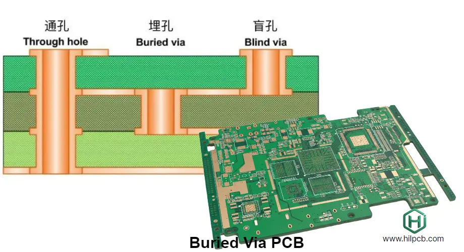
- A buried via PCB should be reviewed as a multilayer routing and fabrication decision, not as a default "high-end" upgrade over standard through-via structures.
- The first checks are whether buried vias actually solve a routing problem, how they fit the stackup, how many lamination or drilling steps they introduce, and whether the added process burden is justified by density or electrical performance.
- Buried vias connect only internal layers, so they can help free outer-layer routing area and reduce some stub-related compromises, but they also add fabrication complexity and inspection difficulty.
- IPC board-design guidance for HDI and complex multilayer structures matters here because buried vias are valuable only when the stackup, registration, test strategy, and yield expectations are aligned.
- Most failures come from overusing buried vias where simpler structures would work, releasing a stackup before the process is frozen, or underestimating how sequential fabrication choices affect cost, yield, and lead time.
A buried via is an internal plated interconnection between inner layers of a multilayer PCB. It does not reach the external board surfaces. The key engineering question is not whether buried vias sound advanced, but whether they improve routing density or electrical behavior enough to justify the added manufacturing complexity and reliability risk.
Contents
- What to review first on a buried via PCB
- Key design and validation rule table
- Early trade-off table
- How stackup, routing, and fabrication choices affect buried via value
- How reliability and release planning should be handled
- What teams should freeze before prototype release
- FAQ
- Next steps
- References
- Author and review
What to review first on a buried via PCB
Buried vias are often requested when a board becomes dense, but density alone is not enough justification. The real question is whether buried vias improve the routing and electrical problem more efficiently than a simpler through-via or blind-via structure.The first review points are usually:
- which layer-to-layer connections actually benefit from being internal only
- whether the routing problem can be solved with ordinary multilayer planning before moving to buried structures
- whether the stackup and fabrication path already assume sequential lamination or multiple subcomposite steps
- whether the board also includes blind vias, microvias, or HDI build-up that change the best buried-via strategy
- whether the project is cost, lead-time, or yield sensitive enough that a simpler structure may be preferable
For teams still defining the base construction, it is usually worth reviewing multilayer PCB, HDI PCB, and Gerber viewer checks together before layout release.
Key design and validation rule table
| Rule / parameter | Recommended range or decision method | Why it matters | How to verify | If ignored | | --- | --- | --- | --- | --- | | Buried-via need | Use buried vias only where they solve a real routing or electrical problem | Added process steps are only justified by real board-level benefit | Stackup and fanout review | Complexity rises with little value | | Stackup integration | Define which inner layers are connected before routing spreads | Buried vias only work cleanly when layer use is planned intentionally | Stackup review and fabricator review | Internal connections become ad hoc and hard to build | | Sequential build path | Freeze drilling and lamination sequence early | Buried vias affect process count, yield, and cost directly | Fabrication-flow review | Quote, lead time, and DFM diverge late | | Test and inspection path | Decide how internal interconnect quality will be verified | Buried vias are harder to inspect than surface-visible structures | Electrical-test plan and microsection review | Internal defects are harder to catch and explain | | Combined-via strategy | Align buried vias with through vias, blind vias, or microvias as one system | Mixed via families create different registration and reliability challenges | Pad-stack review and layout review | The board is dense but process assumptions conflict | | Reliability margin | Match buried-via use to product stress and expected lifecycle | Internal structures still depend on lamination and plating quality | Reliability review and supplier capability review | Field margin is assumed, not demonstrated |Early trade-off table
| Design choice | Usually stronger for | Main trade-off | What to confirm early | | --- | --- | --- | --- | | Standard through-via multilayer | Lower complexity and easier inspection | Outer-layer routing area is consumed | Whether density is still manageable | | Buried vias in selected inner connections | Better inner-layer connectivity and preserved outer routing | More fabrication steps and internal-process burden | Real routing benefit | | Blind plus buried combination | Stronger escape routing on denser boards | Higher registration and process complexity | Whether HDI is truly required | | HDI microvia approach | Very dense package fanout | Different process family with its own risk set | Whether buried vias or microvias solve the real problem better |How stackup, routing, and fabrication choices affect buried via value
Buried vias are valuable only when they improve the total board solution. If they are added by habit, they usually make the board more expensive and less forgiving without solving the actual bottleneck.Three review questions usually matter most.
1. Do buried vias free meaningful routing space?
If inner-layer-only connections let the outer layers stay cleaner for escape routing, controlled interfaces, or connector fields, the added complexity may be worth it. If not, simpler structures are often better.
2. Is the stackup built around the buried-via plan from the start?
Buried vias are not a late decorative feature. They affect subcomposites, lamination order, drilling stages, and test assumptions. IPC board-design guidance for HDI and multilayer structures matters because stackup discipline is what keeps these features manufacturable.
3. Is the board choosing the right via family overall?
Some designs are really microvia or blind-via problems, not buried-via problems. That is why PCB viewer and Gerber viewer review matters. The cleanest construction is often the one that solves just enough routing pain without escalating process count more than necessary.
How reliability and release planning should be handled
Buried vias should be released like a fabrication strategy, not just like a layout feature.The practical checks are:
- verify the intended fabricator supports the actual lamination and inner-layer registration flow
- define how internal interconnects will be checked through electrical testing, coupons, or microsection evidence
- align buried-via use with product reliability expectations rather than assuming all multilayer boards face the same stress
- confirm that quote, lead-time, and yield assumptions are based on the real stackup rather than a simplified RFQ label
If the board is still early in DFM, PCB prototype, quick-turn PCB, and HDI PCB planning often reveals whether buried vias are genuinely needed or whether a simpler routing strategy will close the design faster.
What teams should freeze before prototype release
Buried-via projects become expensive when the board is quoted before the internal build path is agreed.A practical release checklist usually includes:
- Buried-via scope approved
Freeze which layer pairs use buried vias and why they are needed. - Stackup and fabrication flow approved
Lock lamination order, drilling sequence, and mixed-via assumptions before final release. - Inspection and test path defined
Decide what electrical test, coupon, or microsection evidence will be used to verify internal quality. - Combined-via strategy aligned
Confirm how buried vias interact with through vias, blind vias, or HDI structures on the same board. - Prototype objective written
Define whether the first build is proving routing feasibility, fabrication stability, or lifecycle reliability.
If the design is still moving quickly, PCB prototype and quick-turn PCB support usually shortens the loop between stackup decisions and manufacturable release.
FAQ
What is the first thing to check before using buried vias?
Start by asking whether buried vias solve a real routing or electrical problem that simpler structures cannot solve cleanly.
Are buried vias always better than through vias?
No. They can preserve routing space and help certain stackups, but they also increase fabrication complexity, inspection burden, and cost.
Do buried vias automatically mean the board is HDI?
Not automatically. Some buried-via boards are complex multilayer designs without full HDI build-up, while some HDI boards combine buried vias with blind vias or microvias.
Why must the fabrication path be frozen early?
Because buried vias change inner-layer construction, lamination sequence, and verification strategy. If those are vague, the layout and quote stop matching each other.
What should be frozen before prototype release?
Freeze the buried-via scope, stackup, fabrication flow, inspection path, mixed-via strategy, and the real objective of the prototype build.
Next steps
If you are evaluating buried vias for a dense multilayer design, the most useful next step is usually to review routing benefit, stackup, lamination flow, and verification path as one fabrication decision before sending the board to quote.HILPCB can support that process through:
- Multilayer PCB planning for complex internal routing structures
- HDI PCB review when buried vias interact with blind vias or microvias
- PCB prototype and quick-turn PCB for early stackup validation
- Gerber viewer and PCB viewer checks before fabrication release
- Request a quote when your stackup and process assumptions are ready