
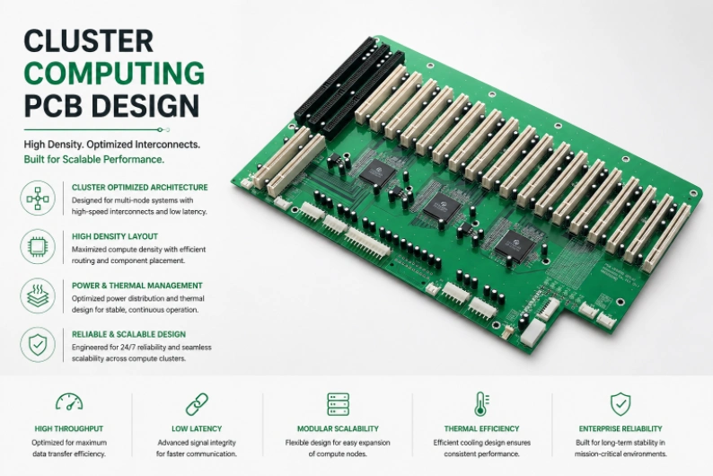
The global HPC cluster market exceeded $49 billion in 2024, with enterprise AI training and scientific simulation driving demand for tighter node integration, faster interconnect bandwidth, and GPU-dense configurations that push blade PCB design to its limits. Cluster computing connects co-located nodes through high-bandwidth, low-latency interconnects — enabling tightly-coupled parallel workloads where nodes exchange data every millisecond during MPI barrier synchronizations, all-reduce operations, and neighbor exchanges in stencil computations.
The critical distinction between cluster computing and loosely-coupled distributed systems is communication intensity. A CFD simulation running across 512 cluster nodes performs MPI_Allreduce operations involving every node thousands of times per second — each synchronization waiting for the slowest node to complete. An AI training job performing data-parallel gradient averaging across 256 GPU nodes executes all-reduce operations after every mini-batch, with network latency directly adding to training iteration time. This communication intensity means the interconnect path — and the PCB carrying it — determines whether adding nodes improves performance or creates overhead.
HILPCB manufactures cluster computing PCBs including 500 mm blade-format boards with 0.2% flatness tolerance, InfiniBand HDR/NDR adapter cards, and midplane/backplane assemblies — for system integrators building HPC and AI training clusters across North America, Europe, and Asia-Pacific.
Menu Navigation
- Interconnect-First Node Architecture
- InfiniBand HDR/NDR and High-Speed Ethernet Routing
- Blade Form Factor: Routing in a 30×500 mm Corridor
- Multi-Kilowatt Power Distribution for GPU-Dense Blades
- Reliability for Non-Stop Cluster Operation
- Integrated Blade and Midplane Manufacturing
Interconnect-First Node Architecture
Modern cluster nodes are built around server-class CPUs or GPU accelerators, supported by 8–12 DDR5 channels, PCIe Gen 5 expansion, and 200G/400G InfiniBand or Ethernet interconnect. The critical design philosophy differentiating cluster boards from general server boards is interconnect priority — the network interface receives the shortest PCIe path, the best signal integrity routing layers, and the most favorable thermal position before any other subsystem.In a standard server, the network interface is one of many peripherals competing for PCIe lanes and board routing resources. In a cluster node designed for MPI communication, the network interface operates at wire rate continuously — 400G InfiniBand NDR sustains 50 GB/s bidirectional bandwidth without the idle periods that cloud servers experience between independent requests. This sustained utilization profile means any signal integrity deficiency on the network path directly limits the cluster's aggregate computational throughput.
Cluster-Specific Design Priorities
- Interconnect-First PCIe Allocation: Network HCA (Host Channel Adapter) or SmartNIC placed on PCIe Gen 5 x16 lanes routed directly from CPU root complex — the shortest, lowest-loss, lowest-latency PCIe path on the board. Storage and peripheral devices receive remaining PCIe lanes through switch or downstream ports.
- Multi-Channel DDR5 for Data-Intensive MPI: 8–12 DDR5 channels routed with ±1 mil byte-lane matching on high-speed PCB layers — supporting maximum memory bandwidth for MPI buffer operations where message packing/unpacking performance is memory-bandwidth-limited.
- GPU Accelerator Integration: PCIe Gen 5 x16 slots for 4–8 GPU accelerators with power delivery supporting 500W+ per card through heavy copper distribution from 48V backplane power — GPU-equipped cluster nodes dissipate 2,000–4,000W total, requiring power delivery infrastructure that exceeds standard server design.
- Midplane Connector Interface: Board-edge connector footprints precisely matching chassis midplane specifications with impedance continuity maintained through the board-to-connector transition — verified through S-parameter measurement of the mating interface during first-article qualification.
InfiniBand HDR/NDR and High-Speed Ethernet Routing
MPI communication latency directly determines cluster application scaling efficiency. The PCB network path — from CPU PCIe root complex through board traces, via transitions, and connector to the network HCA SerDes — contributes directly to every MPI operation's latency and determines the maximum achievable fabric bandwidth.InfiniBand NDR at 400G per port uses 4 lanes of 100G PAM4 signaling — each lane operating at the same data rate that required ultra-low-loss materials and precision fabrication only 3 years ago for the most demanding switch boards. Now this signal integrity requirement applies to every cluster node board in the system.
Interconnect Signal Integrity
- InfiniBand NDR 400G Routing: 4 lanes × 100G PAM4 per port with insertion loss below 4.5 dB at 26.5 GHz Nyquist — achieved through low-loss laminates (Df < 0.003 at 15 GHz), HVLP copper foil (Rz < 2.0 μm), and via stub elimination through back-drilling or blind via construction on all layer transitions.
- GPU-Direct RDMA Path Optimization: Direct PCIe routing from GPU slot to NIC with minimal hop count (zero PCIe switch traversals) and consistent impedance through all transitions — enabling GPU-to-GPU communication across nodes at 400G wire rate without CPU involvement, critical for NCCL/RCCL collective operations in distributed AI training.
- Deterministic Latency Through Hardware Path: Impedance discontinuities and via stub resonances create inter-symbol interference that manifests as data-dependent latency variation — increasing 99th-percentile tail latency that becomes the bottleneck for MPI barrier synchronizations where the slowest communication determines system-wide wait time.
- Production Eye Diagram Verification: Channel quality verified through eye diagram measurement at 100G PAM4 data rates on first-article boards — not just TDR static impedance measurement, which misses frequency-dependent loss mechanisms that dominate at PAM4 data rates.
Blade Form Factor: Routing in a 30×500 mm Corridor
Blade servers maximize compute density — a 10U chassis accommodating 16–20 blades, each containing a complete compute node on a PCB constrained to approximately 30 mm width and up to 500 mm length. This extreme aspect ratio (16:1 or higher) creates routing and thermal challenges fundamentally different from standard server motherboard design.Blade-Specific PCB Design Challenges
- Length-Dominated Signal Routing: All high-speed signals traverse the full 400–500 mm board length — DDR5 command/address buses extend 100–150 mm, PCIe x16 lanes run 200+ mm to the backplane connector, and power rail routing spans the entire board. These lengths consume insertion loss budget aggressively — standard FR-4 with Df 0.020 at 10 GHz creates 6+ dB loss on DDR5 routes that exceeds timing margin, forcing low-loss material selection even for interfaces that work on standard FR-4 in wider board formats.
- Backplane Connector Mechanical Integration: Blade-side connector footprints fixed by chassis specification (typically PICMG 3.0 or proprietary) — PCB layout must hit exact pin positions within ±2 mil while maintaining differential pair impedance through the board-to-connector transition zone on multilayer constructions of 16–24 layers.
- Confined Thermal Extraction: 30 mm blade spacing limits heatsink height to 15–20 mm with minimal cross-flow airflow. Heat extraction relies on board-edge thermal interfaces (copper thermal bridges conducting to chassis cold rails) and bottom-side contact pads — heavy copper inner planes (2–3 oz) provide essential lateral heat spreading from concentrated die footprints to edge-mounted thermal bridges.
- Warpage Control at Extreme Aspect Ratio: Long, thin blade boards are inherently warpage-prone — the length-to-width ratio amplifies any copper distribution asymmetry. Symmetric copper distribution across all layers and balanced lamination sequence maintain flatness within ±0.2% of diagonal — critical for reliable backplane connector mating and consistent thermal interface contact.
Multi-Kilowatt Power Distribution for GPU-Dense Blades
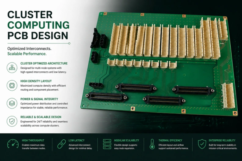
GPU-equipped cluster blades represent the highest power density in any computing form factor — a blade with 2 CPUs and 4 GPU accelerators draws 2,500–4,000W from 48V backplane power, all converted to multiple sub-1V voltage rails within the blade PCB footprint. A 10U chassis with 16 such blades concentrates 40–64 kW in less than half a rack — power density exceeding most commercial electronics by an order of magnitude.Blade Power Architecture
- 48V Direct-to-Load Conversion: Two-stage architecture (48V→6V intermediate bus + 6V→Vcore multiphase buck) reducing distribution losses by 4–6× versus 12V bus. 48V routing on dedicated power layers with appropriate creepage distance (>0.5 mm for functional insulation per IEC 62368-1) and switching transient management for 48V half-bridge converters switching at 300–500 kHz.
- Active Current Sharing Between Redundant Inputs: Redundant 48V feeds from the midplane with active current balancing — maintaining seamless power continuity during N+1 power module failures without voltage transients that would reset processors or corrupt in-flight computation.
- Voltage Droop Compensation Under GPU Transients: GPU kernel launch creates 200–300 A/μs current transients from idle-to-full-load — load-line impedance calibrated to compensate for PCB IR drop, maintaining voltage regulation at the processor die pad within ±5 mV throughout the transient event.
- Per-Rail Power Telemetry: Shunt-based current sensing (±1% accuracy) and voltage monitoring on every major rail — feeding data to BMC for rack-level power management, thermal policy enforcement, and predictive maintenance through anomaly detection on power consumption patterns.
Reliability for Non-Stop Cluster Operation
Cluster nodes run continuously for years. Unscheduled maintenance on a single node forces running MPI jobs to checkpoint, evacuate the failed node, and restart — a process that can waste hours of compute time across hundreds of nodes for a large-scale simulation. Making field reliability the dominant total cost of ownership factor for cluster computing installations.Cluster Reliability Framework
- Extended Component Qualification: Electrolytic capacitors derated 30% in voltage and 20% in temperature above rated limits, MLCC specified as X7R minimum (C0G for timing-critical circuits), and MOSFETs with thermal Rdson maintaining 25% margin above maximum steady-state current at worst-case junction temperature.
- SMT Assembly for Extended Life: SAC305 solder joints qualified through 3,000+ thermal cycles per IPC-9701 at the blade's actual operating temperature range — 3× the standard 1,000-cycle qualification, validated through cross-section analysis and pull/shear testing after cycling.
- Predictive Failure Detection: BMC sensor interfaces monitoring VRM phase currents, capacitor ESR (through impedance measurement), DIMM error rates (through ECC counters), and thermal trending — enabling scheduled replacement of degrading components before failure during planned maintenance windows.
- Field-Serviceable Architecture: Modular board design with accessible test points for on-site diagnostics using standard multimeter and oscilloscope — enabling tier-2 field technicians to identify failed subsystems without shipping boards back to the manufacturer.
Integrated Blade and Midplane Manufacturing
Cluster programs follow structured build sequences — 5–10 board bring-up runs for firmware development, 50–200 board pilots for system integration, and 500–10,000+ production builds for customer deployment. The unique manufacturing challenge of cluster computing is that blade PCBs and midplane/backplane PCBs must be fabricated together with coordinated dimensional control, because connector mating between blade and midplane depends on both boards meeting their respective tolerance specifications simultaneously.Coordinated Production
- Prototype Bring-Up: 5–10 blade boards and matching midplane sections delivered in 5–7 working days with full component sourcing — enabling simultaneous blade firmware development and midplane integration testing.
- Midplane Co-Fabrication: Both blade PCBs and midplane/backplane boards manufactured with coordinated connector alignment verification — multilayer backplane boards (up to 40+ layers) with press-fit connector holes at ±1.5 mil position tolerance, verified against mating blade connector footprints.
- Turnkey Scaling: Automated assembly with ICT, boundary scan, functional test, and burn-in — maintaining blade-to-blade consistency across production lots spanning months of customer deployment.
- System-Level Connector Verification: Mating force measurement and contact resistance verification on blade-midplane connector pairs — ensuring reliable electrical connection across the 50,000+ insertion cycles expected during the system's service life.
Cluster Computing PCB FAQ
Why do blade server PCBs face extreme routing challenges?
Blade server PCBs have an extreme aspect ratio (e.g., 30x500 mm), meaning high-speed signals like PCIe x16 or DDR5 must traverse long distances. This length aggressively consumes the insertion loss budget, forcing the use of ultra-low-loss materials and precise impedance control to maintain signal integrity from the CPU to the backplane connector.
How is power delivery managed on GPU-dense cluster blades?
A cluster blade with multiple GPUs can draw 2,500-4,000W. To manage this efficiently, boards use a 48V direct-to-load conversion architecture with intermediate bus converters, routed on dedicated heavy copper power layers to minimize IR drop and handle high current transients during GPU load spikes.
Why must blade PCBs and midplane PCBs be co-fabricated?
Reliable connection between a blade and a midplane relies on precise connector alignment. Co-fabricating both boards ensures that the blade connector footprints and midplane press-fit holes meet coordinated dimensional tolerances, guaranteeing secure mating and electrical continuity.
Begin your cluster system PCB program — request a blade board assessment →