
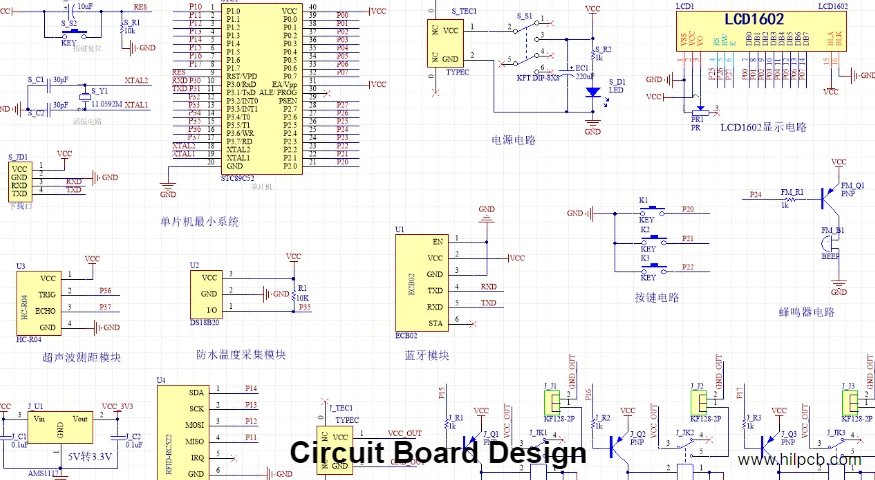
Hi everyone—I'm the lead instructor at HILPCB Design Academy. After years in PCB design and manufacturing, one truth keeps proving itself: in a great PCB, about 80% of success is decided by Component Placement. A well-thought-out component placement strategy is like a city master plan—it determines the smoothness of signal “highways”, the stability of the power network, and the harmony among functional zones. A poor placement, on the other hand, triggers endless Signal Integrity (SI), Power Integrity (PI), and EMC issues, making routing feel like fighting uphill.
This tutorial starts from zero and helps you build a systematic component placement strategy from concept to a manufacturable layout. We’ll cover stackup planning, functional partitioning, key routing strategies, and—based on HILPCB’s manufacturing experience—ensure your design is not only electrically strong, but also manufacturable and cost-effective.
Three fundamental questions to answer before your component placement strategy
Before dragging the first component, great engineers think like detectives and clarify three core constraints. Together, these define the boundaries and foundation of your placement strategy.
Electrical Constraints: This is the center of the design. Identify which nets are “VIPs”. Do you have differential pairs that need 50Ω impedance control? Noise-sensitive analog signals? Or high-current power paths? Once you identify the critical nets, you must reserve the shortest and most direct physical paths and plan the corresponding reference planes. For example, a solid
clock tree layout tutorialwill emphasize that the physical positions of the clock source, PLL, and endpoint devices must be fixed first to minimize jitter and skew.Mechanical Constraints: A PCB does not live in a vacuum—it must fit into a specific enclosure. Board outline, mounting holes, connector orientations and positions (USB, HDMI, etc.), and component height limits are non-negotiable “hard rules”. Lock these mechanical elements precisely at the very beginning; they become the “anchors” of your placement.
Thermal Management Constraints: Heat is the enemy of electronics. Identify major heat sources such as CPU, FPGA, power MOSFET, or LDO. An effective
component placement strategyplaces these “hot components” where heat can be removed (near a fan or enclosure vents), and leaves enough spacing to avoid thermal crowding. Planning thermal pads and sufficient thermal vias is also essential for long-term reliability.
Stackup and reference-plane planning steps
Stackup is the “skeleton” of a PCB. It directly determines impedance-control accuracy, return-path quality, and EMC performance. With a bad stackup, even the best placement can’t save the design.
Key concept: why reference planes matter
High-speed return current always chooses the lowest-impedance path—typically on the reference plane directly beneath the trace (usually a GND or VCC plane). A complete, continuous reference plane is the foundation of signal quality. Any signal crossing a split in the reference plane forces a detoured return path, causing serious EMI radiation and signal distortion. Therefore, when planning stackup, it is critical that every high-speed signal layer is adjacent to a solid reference plane. This is also the first principle a good split plane design guide will stress.
Below is a practical stackup-planning workflow. You can simulate it using HILPCB’s online impedance calculator:
| Step | Core goal | Checklist |
|---|---|---|
| 1. Decide layer count | Choose the right layer count based on signal density, BGA pin count, and impedance-control needs. | Is 4-layer enough? Do you need to move to 6 or 8 layers of [multilayer PCB](/products/multilayer-pcb) for better shielding and power distribution? |
| 2. Assign layer functions | Match signal layers with power and ground layers. A classic rule is “signal adjacent to reference plane”. | Is each high-speed signal layer adjacent to a GND plane? Are power and ground paired to form plane capacitance? |
| 3. Select material and dielectric thickness | Choose materials (FR-4, Rogers, etc.) based on frequency, data rate, and cost. Dielectric thickness directly affects impedance. | HILPCB offers 30+ material options. Does your choice meet the requirements? Are dielectric constant (Dk) and dissipation factor (Df) appropriate? |
| 4. Simulate and confirm | Use tools to calculate trace width/spacing to meet target impedance (50Ω single-ended, 90/100Ω differential). | Submit the stackup to HILPCB for DFM review and get manufacturing suggestions plus an impedance simulation report. |
Component placement and functional partitioning
This is the core execution phase of component placement strategy. The key ideas are “divide and conquer” and “follow the natural flow”.
Functional partitioning: On a whiteboard or in your EDA tool, divide the PCB into logical zones:
- Power zone: DC-DC, LDO, etc., typically placed near the power input connector.
- Digital core zone: CPU, FPGA, DDR memory—this is the center of high-speed signals.
- Analog/sensitive zone: ADC, DAC, op-amps—keep away from digital noise sources.
- Interface zone: USB/Ethernet/display connectors and their protection devices.
- RF zone (if any): antenna, filters, PA, etc.—requires strict isolation and impedance matching.
Signal flow: Place modules and components along the natural path of signals—from input to processing to output. This naturally leads to shorter routes, less delay, and fewer crossings. For example, an ADC should sit close to the sensor input interface, while the MCU belongs near the center of the processing chain.
Prioritization:
- Step 1: Place mechanical fixtures and connectors.
- Step 2: Place core ICs such as the processor and memory. This is the “sun” of the layout; other parts orbit around it.
- Step 3: Place closely related peripheral circuits such as crystal oscillators and PMICs. A good
clock tree layout tutorialwill tell you the crystal must be as close as possible to the MCU clock pin. - Step 4: Place decoupling capacitors. Put them tight to each IC power pin—this is the golden rule of PI.
- Step 5: Place the remaining supporting components.
Differentiated strategies for high-speed / power / analog routing
Placement sets the ceiling for routing. A good placement makes routing dramatically easier. During placement, you should already reserve “corridors” for different signal types.
Planning workflow for routing strategy
- Power nets first: Plan the distribution of main power and ground first. Use a star topology from the power module to each functional zone to avoid current loops. For high-current paths, reserve sufficient copper width or use plane layers.
- Critical high-speed signals: Reserve clear, unobstructed paths for differential pairs, clocks, etc. Think about how they travel from source to load; avoid layer swaps and vias as much as possible. This is key to successful [high-speed PCB design](/products/high-speed-pcb).
- Sensitive analog signals: Plan a dedicated area for analog signals, far from digital noise. Consider using guard trace design—ground traces along both sides of sensitive signals to add shielding.
- Via strategy: Vias enable layer transitions, but also introduce impedance discontinuities. A practical via selection tutorial suggests: for high-speed signals, minimize via size and remove unused stubs; on power/ground planes, ensure a clean return path and avoid placing vias on splits in the reference plane.
Combined checks: DRC + SI + PI
When placement is mostly done, do not rush into routing. This is the best time for preliminary verification and review. A detailed design review checklist pcb is your best friend.
| Category | Key checks | Tools / method |
|---|---|---|
| DRC (physical rules) | Component clearance, silkscreen overlap, and keep-out rules. | Built-in DRC checker in the EDA tool. |
| SI (Signal Integrity) | Are critical paths too long? Is there crosstalk risk? Are reference planes continuous? | Visual review and advanced SI simulation tools. |
| PI (Power Integrity) | Are decoupling capacitors close enough? Are power paths wide enough? Are there improper power-plane splits? | Visual review and advanced PI simulation tools. |
| DFM (manufacturability) | Are components too close to the board edge? Is BGA fanout reasonable? Are test points reserved? | HILPCB’s free DFM review service. |
This design review checklist pcb should be used throughout the project—especially at the two key checkpoints: after placement and after routing.
How to prepare design files and manufacturing deliverables
A perfect design must ultimately be delivered to the manufacturer with a standardized documentation package. Incomplete or unclear files are a top cause of delays and production mistakes.
Core deliverables:
- Gerber Files: Separate files for each copper layer, solder mask, silkscreen, drill layer, etc.
- NC Drill File: Drill coordinates and hole sizes.
- Pick and Place (PnP) File: Also called centroid file; includes coordinates, rotation, and side for each component for automated placement.
- Bill of Materials (BOM): Lists reference designators, part numbers, packages, quantities, and descriptions—this is the “soul” of turnkey PCBA service.
- Assembly Drawing: Clearly marks reference designators and orientations, especially for polarized parts.
- Fabrication Notes: Stackup, impedance requirements, materials, surface finish, and special process requirements.
Before submitting, double-check that BOM matches the schematic and PCB exactly. A tiny error can trigger wrong procurement and major losses.
Iteration with HILPCB design reviews and mass-production feedback
Combining theory with real manufacturing feedback is the fast path to becoming an expert. Working with an experienced manufacturer like HILPCB can dramatically accelerate your growth.
Manufacturing capability that empowers design
Our value is not only in building boards, but also in feeding manufacturing knowledge back into design. Through our free DFM (Design for Manufacturability) review, engineers check whether your placement has potential manufacturing risks—such as dense BGA fanout, poor via design (often not covered in a via selection tutorial), or bad practices from a split plane design guide that could create opens/shorts. We also provide impedance test reports and microsection analysis, so you can directly see whether design intent matches the real product—and optimize your component placement strategy in the next iteration.
Collaboration loop:
- Design phase: Apply the principles in this tutorial and use our online tools for initial checks.
- Before build: Submit your package to HILPCB for full DFM and engineering review. Our engineers provide specific, actionable suggestions.
- In production: We manufacture strictly to the confirmed stackup and impedance requirements, and validate impedance accuracy using coupons.
- After delivery: Review the physical boards and test reports. What worked well? What placement decisions can be improved? These learnings become the foundation of your next revision.
Summary
Building a systematic component placement strategy is the milestone from beginner to experienced PCB engineer. It requires you to be more than a circuit designer—you must be a system architect balancing electrical, mechanical, thermal, and manufacturability factors. Remember: placement first, modularize, follow signal flow, and always keep manufacturability in mind. With continuous practice, reviews, and iteration, your PCB design level will keep rising.
Conclusion
In summary, this article explains PCB design thinking, stackup planning, routing strategy, and DRC checks through the lens of component placement strategy, with printable checklists and examples to help beginners ramp up quickly. By following the checklists and process windows, and involving HILPCB’s DFM/DFA team early, teams can accelerate prototype builds and volume production while maintaining quality and compliance.
Common Questions
Why is component placement strategy so important in PCB design?
Placement decisions influence routing difficulty, signal quality, thermal behavior, EMI risk, manufacturability, and test access before detailed routing even begins. A strong placement strategy therefore sets the foundation for the entire board.
Why should placement be planned together with stackup and reference planes?
Component grouping and orientation determine where critical nets travel and how cleanly they can reference planes. Planning placement without stackup context often creates routing compromises that are harder to fix later.
Why do high-speed, power, and analog circuits need different placement priorities?
Each domain has different sensitivity to noise, current flow, heat, and coupling. A good placement strategy recognizes those differences and partitions the board so each circuit type can perform well without creating avoidable interference.
Why is manufacturing feedback valuable when refining component placement?
Factory feedback can reveal assembly congestion, fanout difficulty, via issues, and other practical limits that are not obvious from the schematic alone. Using that feedback early helps teams improve both buildability and long-term board quality.