
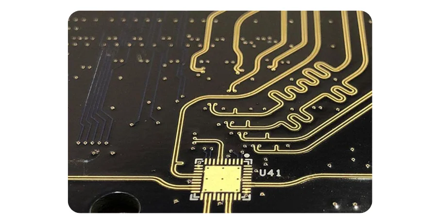
Controlled impedance is affected by copper geometry, dielectric thickness, laminate properties, fabrication tolerances and the measurement method. A passing coupon measurement at shipment does not automatically demonstrate electrical stability for a product’s entire service life.
For high-reliability uses such as aerospace, medical or telecommunications equipment, specify the intended electrical channel, allowable tolerance and required verification. Environmental durability and complete-device reliability need separate evidence; impedance control is one element of the design.
For a HilPCB PCB Factory (HILPCB) quotation, identify the controlled nets, target impedance, stackup and acceptance method. Manufacturing control can reduce variation in the released construction; the product owner must separately establish channel performance and environmental qualification.
Advanced Manufacturing Process Control
HILPCB controls impedance production with continuous process monitoring, sensors, SPC and environmental controls. Every substrate material lot undergoes comprehensive characterization including dielectric constant measurement, loss tangent evaluation, and thermal expansion coefficient testing. HILPCB links the material-lot certificate to the production build. AS9100 and ISO 13485 quality systems apply only to their current certified entity/site and scope. We provide custom impedance manufacturing, DFM, stackup and modeling, plus SMT/flex integration and TDR/VNA, environmental and accelerated-aging analysis. Each controlled-impedance production lot is linked to material, process and coupon reports, calibration traceability and customer quality records; report contents follow the contracted test plan.
Control the variables that materially affect the specified transmission-line construction, and agree how finished geometry and electrical results will be checked.
Process monitoring: Fabricators should control finished copper thickness, etch geometry, laminate thickness and registration using an agreed process-control plan. The customer should verify the measurement and reporting scope before relying on real-time feedback claims.
Material traceability: Request approved laminate specifications, lot identification and available supplier test certificates. Directly measuring Dk, Df and CTE for every material lot is not a default PCB-factory service; confirm any additional characterization in the quotation.
Environmental controls: Temperature, humidity and contamination can affect storage, processing and measurement. Define relevant process conditions and material handling rather than assuming an unspecified environmental system proves long-term electrical stability.
Statistical process control: Select measurable process characteristics and investigate trends against documented limits. Capability indices require a suitable, stable process and measurement system; they do not prove that every board or unmeasured variable meets the design.
Specify the structure, material model and coupon together
A nominal impedance target is not a trace-width specification. A surface microstrip, an embedded stripline and a grounded coplanar line have different field distributions. Define signal layer, reference conductors, finished trace width/thickness, dielectric spacing, and differential spacing where applicable. Include solder mask for a coated surface line and nearby copper where it affects the field. A differential pair's impedance is not generally twice the isolated single-ended value because coupling changes the result.
A laminate's nominal Dk is tied to a grade, construction, frequency and measurement method. Supplier process or specification Dk is not automatically the appropriate solver input. Rogers' discussion of material Dk and design Dk explains how test configuration and circuit-based extraction can produce different values. Agree the model with the fabricator and material supplier; do not infer a generic FR-4 value or treat design Dk as a guarantee for every geometry and frequency.
| Release input | Condition to agree | Acceptance implication |
|---|---|---|
| Impedance target | Single-ended or differential, target and tolerance, controlled nets and layers | A tolerance applies to the stated structure and test method, not every channel parameter |
| Material and stackup | Exact grade/construction, cured dielectric thickness, relevant Dk/Df data and copper | Substitutions or stackup changes need review, even when nominal Dk matches |
| Finished geometry | Etch profile, copper thickness, reference plane, pair gap and mask where present | Use finished geometry and realistic variation in the solver, not artwork width alone |
| Coupon | Representative layer, construction and geometry; panel location and sampling | A coupon supports process acceptance but does not include every routed via, connector or discontinuity |
| Measurement | TDR setup, reference/calibration, effective rise time, launch treatment, evaluation window and reporting | Results must be compared under the agreed conditions; uncertainty and disposition rules belong in the quality plan |
Tektronix's TDR primer describes the effects of rise time, fixture connections and reflections on interpretation. Evaluate a suitable uniform trace region rather than a connector launch or line end. Agree any fixture removal or de-embedding procedure and retain the waveform or defined summary with coupon and board revision identity.
A passing coupon does not establish channel insertion loss, return loss, crosstalk, skew or receiver margin. Use the relevant simulation, S-parameter measurement or system test for those requirements, including actual vias and connectors where they matter.
Aerospace and Defense Manufacturing Standards
Aerospace and defense applications represent the pinnacle of controlled impedance requirements, where performance margins are minimal and failure consequences extend far beyond financial considerations.
Space-material selection: High-Tg laminates can improve processing margins, but Tg alone does not qualify a board for vacuum, radiation or temperatures from −180°C to +150°C. Use application-specific outgassing, thermal-cycle and materials evidence.
Military communication systems: Specify the applicable environmental, electrical and documentation requirements for the equipment. Confirm any export-control and controlled-data handling obligations with the responsible parties before transferring project data; they are not an automatic capability of every fabricator.
Radar design: Allowable impedance variation depends on RF topology, loss budget and measurement reference planes; ±1% across a wide frequency range is not a general manufacturing requirement.
Avionics Integration: Commercial and military avionics utilize controlled impedance PCBs for flight-critical communication and navigation systems. Multilayer PCB designs integrate multiple impedance-controlled layers while meeting stringent weight constraints and shock/vibration requirements.
Aerospace quality: AS9100 is a quality-management standard with organization- and site-specific certification scope. It does not itself certify a controlled-impedance PCB or guarantee aerospace environmental qualification; ask the manufacturer for current certificates and project records.
Medical Device Manufacturing Excellence
Medical devices may use controlled-impedance interfaces where channel requirements justify them. Product risk, patient contact and the finished-device architecture determine applicable regulatory and biocompatibility requirements; these do not follow from impedance control alone.
Patient-monitoring electronics: These systems may require impedance-controlled interfaces, but HDI is selected based on package density, electrical routing and manufacturability; not all portable monitors need HDI.
Surgical equipment: PCB materials and finishes must suit the intended cleaning and assembly processes. Autoclave or chemical sterilization suitability requires qualification of the finished exposed product; conventional internal PCB assemblies should not be assumed sterilizable.
Implantable electronics: These require approved device-specific materials, packaging and reliability validation. ISO 13485 concerns the quality-management system; it does not by itself qualify an implantable assembly or prove hermetic sealing.
Diagnostic imaging systems: MRI, CT and ultrasound electronics can require controlled high-speed or RF paths, but their environments differ. MRI magnetic-field compatibility applies to equipment in the relevant field region; it is not a general CT or ultrasound requirement. Specify material, shielding and channel requirements for the actual subsystem.
Medical-device regulations: The legal manufacturer determines the relevant FDA and international requirements for the intended device. A PCB supplier supports the process with specified manufacturing and traceability evidence; PCB fabrication is not an independent FDA product approval.
Telecommunications Infrastructure Solutions
Telecommunications applications demand controlled impedance PCBs maintaining signal integrity across wide frequency ranges while supporting the highest data rates and most demanding reliability requirements.
5G Base Station Architecture: 5G infrastructure utilizes controlled impedance PCBs for both digital processing and RF sections, with frequency ranges extending from DC to millimeter-wave frequencies. These applications require exceptional impedance accuracy with low-loss materials and precise manufacturing tolerances for outdoor installations.
Optical transceivers: Controlled-impedance traces are important for high-speed electrical host interfaces. The link budget and allowable impedance tolerance depend on the specific transceiver and channel, not just an advertised aggregate 100 Gbps rate.
Network backplanes: High-speed backplanes often use rigid multilayer boards and connectors. Rigid-flex construction is an option for selected mechanical constraints, not the default optimal backplane solution.
Subsea electronics: Repeater and control assemblies may need extended mission life and rigorous enclosure protection. Service-life claims should be based on the particular equipment, failure model and qualification plan; a fixed 25-year PCB lifetime cannot be assumed.
Data Center and Computing Infrastructure
Modern data centers rely on controlled impedance PCBs for high-performance computing applications where signal integrity directly impacts processing capability and energy efficiency.
Server Motherboard Architecture
High-performance servers utilize controlled impedance PCBs for processor interfaces, memory connections, and high-speed I/O systems. DDR5 memory implementations require precise impedance control for reliable operation at maximum data rates while supporting error correction and thermal management.
Enterprise Storage Systems
Storage platforms use controlled impedance PCBs for NVMe interfaces and high-speed storage networks. These applications demand consistent impedance control for maintaining data integrity while supporting hot-swap operations and redundant system architectures.
Network Interface Card Design
100GbE and 400GbE network interface cards require exceptional impedance control for maintaining signal integrity in high-density server environments. SerDes applications operating at 50Gbps+ per lane demand manufacturing precision maintaining performance across temperature variations and aging effects.
Supercomputing Applications
High-performance computing clusters utilize controlled impedance PCBs for inter-processor communication and memory interfaces supporting parallel processing workloads. These systems require impedance consistency across thousands of high-speed connections operating synchronously.
Testing and Validation Excellence
A release test verifies the agreed structures under defined measurement conditions. It does not sample every manufacturing variable or establish the entire product lifecycle.
Electrical verification: Agree whether the manufacturer will provide TDR coupon measurements, S-parameter/VNA characterization, or environmental data. These are different services; calibration traceability and uncertainty must be confirmed for the specified instruments.
Reliability verification: Accelerated aging and thermal cycling can reveal selected failure modes, but cannot guarantee decades of impedance stability without a justified model and representative field correlation.
Statistical Quality Control: Production testing follows comprehensive statistical sampling plans balancing testing costs with quality assurance requirements. Control charts track long-term trends while capability studies demonstrate manufacturing process consistency meeting customer requirements.
Traceability records: Confirm which material lots, impedance coupons and process parameters will be recorded and supplied for each order. A supplier database does not automatically provide full device-level traceability.
Environmental tests: Specify the required test method, sample size, cycles, acceptance limits and responsibility. Electrical coupon checks do not replace complete-product environmental qualification.
Where SMT assembly is included, define any populated-board or channel tests separately from bare-board coupon acceptance. Flex PCB constructions can also use controlled impedance; dynamic-flex use additionally requires bend geometry, stackup and cycle-life qualification.
Frequently Asked Questions
What industries require controlled impedance PCB manufacturing?
We serve aerospace, defense, medical devices, telecommunications, automotive, and high-performance computing applications where impedance accuracy directly affects system performance and reliability.
What quality certifications do you maintain for controlled impedance manufacturing?
Current AS9100, ISO 13485 and other certifications must be checked against the legal manufacturer, facility and certificate scope. ITAR registration, where required, is distinct from product qualification and is not assumed for every PCB supplier.
How is long-term impedance stability evaluated?
Material selection, coupon measurements and appropriately designed environmental tests can support a reliability argument, but the product owner must define the service-life model, acceptance criteria and validation plan.
Can you provide custom impedance values for specialized applications?
Custom impedance targets can be quoted where the material, stackup, geometry and tolerance are manufacturable. Measurement method, coupon location, sample scope and reporting must be agreed before build.
What documentation do you provide with controlled impedance PCBs?
Request coupon impedance data, stackup and material information, process records and any calibration certificates as distinct deliverables. The available traceability depends on the agreed quality plan; do not assume all reports are included with every order.
How do you handle design reviews for controlled impedance projects?
Review the proposed stackup, material model, finished geometry, tolerance and coupon with the fabricator before release. Approve any trace-width or material substitution through change control. Modeling and DFM review support the design; they do not guarantee all channel, assembly or lifetime requirements.