
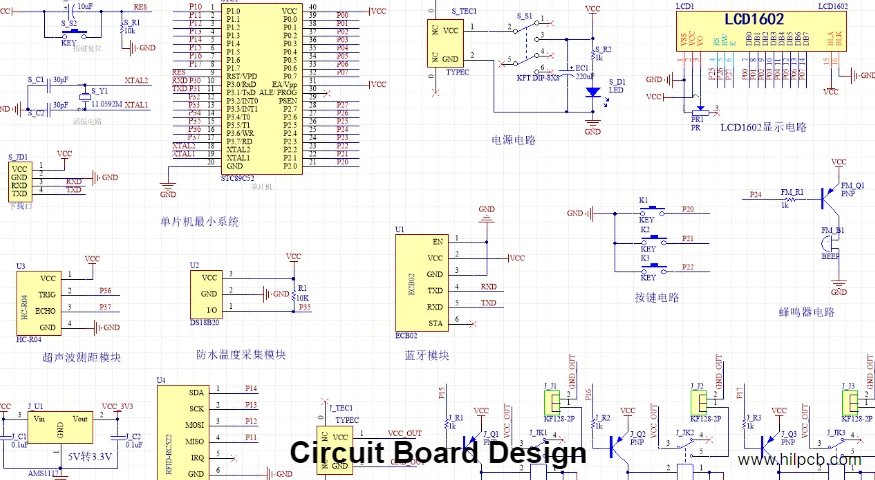
Executive summary: the gap between “design complete” and “manufacturing success”
In today’s high-speed, high-density product development, PCB design is no longer just an “electrical connectivity art.” It is a system engineering process spanning design, simulation, manufacturing, and test. Yet many R&D teams still face the same painful pattern: review processes are missing or superficial, so defects are discovered only after release; engineers rely on individual experience that never becomes a team standard; design and manufacturing information is fragmented, causing constant EQs and revisions that burn schedule and budget. At the root is the lack of a structured, measurable, manufacturing-linked design review checklist PCB system.
This whitepaper from the HILPCB Design Enablement Center provides a complete, practical path for engineering leaders and PCB designers. We cover:
- Process maturity model: assess your current review capability and define a clear upgrade path.
- Front-end planning: how stackup/material/impedance planning prevents 80% of SI and manufacturability issues.
- Modular strategy library: proven placement/routing best practices for high-speed, power, analog, and more.
- Core DFM/DFT checklist: 35+ rules you can apply immediately—from schematic to assembly test.
- Standardized handoff: clear design-to-manufacturing deliverable templates to remove ambiguity.
- Quantified metrics: a measurement system centered on first-pass success to drive continuous improvement.
With this whitepaper, HILPCB aims to help your team upgrade scattered pcb design checklists into a dynamic, closed-loop engineering methodology—enabling true design-manufacturing collaboration and faster, more reliable product launches.
Key takeaways
- Process standardization: Build a full-lifecycle design review framework from requirements to handoff—replacing experience-driven, ad-hoc review.
- Checklist-driven execution: Use a detailed DFM/DFT checklist as the core tool for self-check, peer review, and manufacturing introduction.
- Manufacturing alignment: Bring HILPCB’s capability model into early stackup/impedance/process planning.
- Data closed loop: Use KPIs (FPY, impedance hit rate) and pilot-build retrospectives to continuously improve rules and checklists.
PCB design process maturity model: where are you?
An effective design review checklist pcb does not exist in isolation. It is rooted in your team’s overall process maturity. We define four levels to help you locate your current state and plan a realistic upgrade path.
| Maturity level | Description | Checklist state | Risks & challenges | HILPCB collaboration value |
|---|---|---|---|---|
| L1: Ad-hoc | No unified process; relies heavily on senior engineers’ personal experience. Reviews happen “right before release” and vary each time. | Personal notes or verbal checks; incomplete coverage. | - High rework rate and major schedule risk - Knowledge doesn’t transfer; onboarding is hard - Frequent manufacturing issues; cost out of control |
Provide a basic DFM report to expose obvious manufacturability errors. |
| L2: Defined | Basic Word/Excel templates exist; flow (schematic → placement → routing) is defined; review meetings become routine. | Static checklist based on generic rules, weakly linked to real manufacturing capability. | - Checklist updates lag new processes - DFM checks happen too late; fixes are expensive - Manual review is slow and error-prone |
Provide standardized pcb design checklists templates and introduce online DFM tools for automated first-pass checks. |
| L3: Managed | Process and checklist are standardized and enforced. DFM/DFT are considered early. Key metrics start being tracked. | Dynamic checklist tailored by product type (high-speed/RF/power) and integrated into EDA DRC rules. | - How to ensure strict execution? - How to quantify review impact? - How to feed manufacturing data back into rules? |
Deep collaboration: early stackup/impedance modeling; customized DRC rule packages; validate impedance hit rate via pilot-build TDR reports. |
| L4: Optimized | Design and manufacturing data are connected. Some rules are validated automatically via scripts. Yield data drives continuous rule-library iteration. | A “living” checklist driven by design, manufacturing, and test data—digitized and automated. | - Needs a strong data platform - Requires high cross-team collaboration |
Integrated partner: build a data closed loop and feed pilot/volume yield data back into design to optimize design guideline and enable data-driven design. |
Implementation path: from L2 to L3
- Form a process improvement taskforce: include design, process, and test engineers.
- Baseline the checklist: consolidate scattered lists and combine with HILPCB DFM/DFT templates to form a V1.0 standard checklist.
- Tool integration: configure key physical rules (line width/spacing/vias) into EDA DRC rules.
- Early engagement: require stackup and impedance planning using HILPCB online tools during stackup design.
- Pilot & retrospective: choose one new project as a pilot, enforce the new process, and run a full post-build review to update the checklist.
The foundation of success: stackup, materials, and impedance planning
In any design review checklist pcb, stackup review should come first. Stackup is the “DNA” that determines performance, stability, and manufacturing cost—an incorrect plan cannot be rescued by clever routing later.
Core planning principles
- Reference plane integrity: high-speed signal layers must be adjacent to a continuous reference plane (GND or Power) to control impedance and suppress crosstalk. See ground plane best practices.
- Strong signal-plane coupling: reducing dielectric thickness between signal and reference plane reduces crosstalk and improves EMC.
- Symmetry: keep stackup symmetric to reduce bending/warpage during fabrication.
- Material selection: choose board materials based on data rate/frequency and cost (e.g., FR-4 Tg150, S1000-2M, Rogers RO4350B). Key parameters are Dk and Df.
Common stackup options comparison
The table below compares three typical stackups and the tradeoff between performance and cost. HILPCB can provide custom stackup modeling to achieve impedance-control accuracy better than ±7%.
| Option | Typical structure | Pros | Cons | Best for | Impedance accuracy (HILPCB) |
|---|---|---|---|---|---|
| Standard 4-layer | SIG - GND - PWR - SIG | - Lowest cost - Simple structure |
- Weaker impedance control - Limited EMC performance - Tight routing space |
Low-speed control, simple power products | ±10% |
| High-speed 6-layer | SIG - GND - SIG - SIG - PWR - GND | - Strong SI - Two solid reference planes - Flexible routing |
- Medium cost - Requires disciplined planning |
DDR, PCIe, USB3.0 and other high-speed digital | ±7% |
| RF/mixed-signal 8-layer | SIG - GND - SIG - GND - PWR - SIG - GND - SIG | - Excellent isolation - Independent analog/digital partitioning - Stable impedance control |
- Higher cost - More complex manufacturing |
RF communication, high-speed ADC/DAC, precision instruments | ±5% |
Modular placement and routing strategy library
Efficient placement/routing is key to electrical performance. Instead of reinventing rules per project, build a validated strategy library and standardize handling by circuit module type.
High-speed digital (e.g., DDR3/4)
- Placement: follow daisy-chain or star topology requirements for CPU/FPGA, DDR devices, and termination resistors to ensure timing margins.
- Routing: enforce strict length matching (within data groups and address/clock groups); use differential routing; use HILPCB impedance tools to compute geometry. See high speed trace routing guide.
Power delivery network (PDN)
- Placement: place bulk capacitors near power entry; place high-frequency decoupling capacitors (0.1uF, 0.01uF) as close as possible to IC power pins to minimize loop inductance.
- Routing: use wide copper pours/planes for power paths; avoid thin traces. For multi-rail systems, use star grounding to prevent digital/analog ground contamination.
Analog and mixed-signal
- Placement: physical isolation first—partition analog, digital, and power sections.
- Routing: keep analog away from high-speed clocks and switching supplies. For sensitive analog lines, use guard trace design. Connect analog and digital grounds at a single point (often under ADC/DAC).
Power electronics (e.g., Buck/Boost)
- Placement: minimize HF switching loop area (MOSFET + diode + input cap) to suppress EMI.
- Routing: use ultra-wide copper for high-current paths (input/output/inductor) and consider solder-thieving by opening mask. Use Thermal Vias to conduct heat into bottom heat-spreading planes.
Core DFM/DFT checklist (Design for Manufacturing/Testability)
This is the heart of design review checklist pcb. Run it in phases—after schematic completion, during placement/routing, and before final Gerber release. The table below highlights 35+ critical items; HILPCB automation can cover 90%+ of these rules.
| Category | Rule | Suggested value/spec | Risk | Verification |
|---|---|---|---|---|
| Schematic | ERC check | 0 Errors, 0 Warnings | Incorrect connectivity, functional failure | EDA ERC |
| Footprint match | 100% matches datasheet | Not solderable in production | Manual check, BOM review | |
| BOM completeness | MPN, package, tolerance, refdes complete | Wrong procurement, build stoppage | BOM tools | |
| PDN decoupling | 0.1uF per power pin | Power noise, instability | Schematic review | |
| SI termination | Matching resistors on high-speed signals | Reflections, eye degradation | Simulation, peer review | |
| Placement | SMD spacing | ≥ 20 mil | Difficult soldering, hard rework | DRC, manual check |
| Orientation consistency | Polar parts aligned (diodes/caps) | SMT placement errors | Manual check | |
| Hot component placement | Away from sensitive analog; in airflow | Thermal drift, performance loss | Thermal sim, review | |
| Connector placement | Accessible, matches enclosure | Unassemblable/unusable | 3D model review | |
| Fiducials | 3, non-collinear, > 5 mm from edge | Reduced SMT accuracy | DRC, Gerber review | |
| Routing | Min line/space | By copper (e.g., 1oz: 4/4 mil) | Opens/shorts, low yield | HILPCB DFM, DRC |
| Impedance tolerance | ±10% (standard) / ±7% (tight) | SI issues | HILPCB impedance calculator | |
| Avoid sharp/90° corners | Use 45° or arcs | Acid Trap, impedance discontinuity | DRC, manual check | |
| Via selection/placement | Avoid on pads (unless Via-in-Pad) | Cold solder, paste loss | via selection tutorial, DRC | |
| BGA fanout | Dogbone/teardrop; clear channels | Unroutable, excessive detours | Manual check | |
| Power/ground width | 20 mil/A (rule of thumb) | Excess IR drop, heating | PI sim, review | |
| Remove floating copper | Remove unconnected copper pours | EMC issues, process risk | EDA tools | |
| Planes | Crossing plane splits | High-speed must not cross splits | Broken return path, strong EMI | DRC, manual check |
| Ground integrity | Ensure low-impedance ground | Noise, instability | Review | |
| Thermal relief | Vias/PTH pins in large pours | Hard soldering (over-sinking) | DRC, Gerber review | |
| Silkscreen | Readability | Height > 35 mil, width > 6 mil | Unreadable, debug issues | Gerber review |
| Silkscreen on pads | No silkscreen over SMD/PTH pads | Poor solderability | DRC, HILPCB DFM | |
| Polarity/pin-1 marking | Clear and consistent | Assembly errors | Manual check | |
| Solder mask | Solder mask dam | ≥ 4 mil (fine-pitch IC) | Shorts during soldering | HILPCB DFM |
| Via tenting | Selective tent/open as needed | Test impact or shorts | Gerber review | |
| Fabrication | Annular ring | ≥ 3 mil | Via breakout, reliability risk | HILPCB DFM |
| Edge clearance | Copper/parts ≥ 20 mil from edge | Damage in V-cut/CNC | DRC | |
| Panelization | V-cut, mouse bites, rails | Not SMT-processable | Confirm with HILPCB | |
| Special process notes | Impedance, Via-in-Pad, gold fingers | Wrong manufacturing | FAB drawing | |
| Test (DFT) | Test point coverage | > 90% critical nets | Hard fault isolation | DFT tools |
| Test point pitch | ≥ 1.27 mm (flying probe) | Probe can’t contact | DRC | |
| Test point type | Dedicated test pads | Damage parts/vias | Review |
Design-to-manufacturing handoff template: ensure lossless information transfer
A clear, complete, standardized handoff package is essential for smooth collaboration. Missing or ambiguous information leads to delays. We recommend your design handoff package include at least:
- Gerber files (RS-274X or X2): copper, solder mask, silkscreen, paste, drill layers, etc.
- IPC-356A netlist: for electrical test to ensure no opens/shorts.
- Excellon drill files: hole sizes, coordinates, PTH/NPTH attributes.
- Stackup report: laminate structure, material models, dielectric thickness, copper weights, target impedances and corresponding trace geometry (preferably generated by HILPCB tools).
- Fabrication drawing:
- board outline and tolerances
- stackup diagram
- layer names/order
- finished thickness and tolerances
- surface finish (ENIG, lead-free HASL, etc.)
- solder mask/silkscreen colors
- special processes (impedance table, gold fingers, Via-in-Pad, edge plating, etc.)
- BOM: accurate MPN, package, description, refdes, quantity.
- Pick and place file: SMT centroid coordinates, rotation, and side.
- Test plan (optional): test point location, method (flying probe, ICT), and key limits.
Ready to optimize your design handoff?
Download HILPCB’s standardized handoff template kit (FAB drawing, BOM, Stackup report examples) to ensure your design intent is executed with 100% accuracy.
Build a KPI system: quantify the value of design reviews
To drive continuous improvement of design review checklist pcb, you need measurable KPIs:
- First Pass Yield (FPY): the gold metric for design quality and process effectiveness. Target >95%.
- Number of revisions: number of hardware iterations before mass production—lower means better planning/review.
- Impedance hit rate: based on HILPCB TDR reports, the % of measured impedance within tolerance (e.g., ±7%).
- EQ count: number of manufacturer questions during production—lower means clearer documentation.
- Prototype-to-production cycle time: total time from first prototype to stable mass production.
HILPCB collaboration services: turning checklists into productivity
HILPCB is more than a PCB manufacturer—we help enable your design process. Through a “technology + service + data” approach, we turn design review checklist pcb from a static document into an executable productivity tool.
HILPCB design-manufacturing collaboration capabilities
- Early technical engagement: At project start, our engineers can provide stackup/impedance modeling based on our large material library—building manufacturability into the design from the source.
- Smart DFM/DFA analysis: Upload Gerber to our online platform and receive a detailed report within minutes, covering 100+ manufacturing/assembly rules to reduce human review misses.
- Expert engineering review: For complex high-speed/high-density designs, senior CAM engineers provide 1:1 review and recommendations for SI, PI, EMC, and more.
- Data closed-loop feedback: After each build, we deliver not just boards but data—TDR reports, cross-section analysis, AOI data—so you can improve the next revision and update your internal checklist.
Success story: a leading IoT device maker integrated internal pcb design checklists with HILPCB DFM tools, reducing average prototype iterations from 2.5 to 1.2 and cutting time-to-market by 30%.
Your design review checklist pcb is a key asset for engineering capability, product quality, and faster market response. Let HILPCB be your partner to build this core advantage.
Start your high-reliability design journey now
Contact our technical consultants for a free manufacturability assessment and learn how we can help you build or optimize your team’s design review checklist PCB system.
Common Questions
Why should a PCB design review checklist be built early instead of before release?
Most expensive PCB risks are introduced long before final release, during stackup definition, placement, routing, and handoff planning. Building a design review checklist pcb process early helps teams catch manufacturability, testability, and signal-risk issues before they become costly revisions.
What should always be included in a design-to-manufacturing handoff package?
A solid handoff package normally includes Gerber data, drill files, stackup information, fabrication notes, BOM with manufacturer part numbers, pick-and-place data, and test-related documents when needed. The goal is to transfer design intent clearly enough that manufacturing does not have to guess.
Which KPIs are most useful for improving the review process?
First-pass yield, revision count, impedance hit rate, engineering question count, and prototype-to-production cycle time are practical indicators because they connect checklist quality to real production outcomes. They show whether the review process is actually reducing risk and friction.
When should a PCB manufacturer or DFM team be involved in the review flow?
The best time is before layout decisions harden, especially for high-speed, high-density, or assembly-sensitive boards. Early collaboration with a manufacturer like HILPCB improves stackup planning, rule selection, DFM/DFA feedback, and the quality of the final handoff package.
Conclusion
This article is written for design leads and provides a framework for design review checklist PCB—stackup/routing strategy, DFM/DFT checklists, and handoff templates—to align design and manufacturing and control risk across design, materials, and test. By executing the checklist and process window consistently and engaging HILPCB’s DFM/DFA team early, you can accelerate prototypes and production while maintaining quality and compliance.
For manufacturing and assembly support, contact HILPCB Turnkey Assembly or SMT Assembly for DFM/DFT recommendations.