
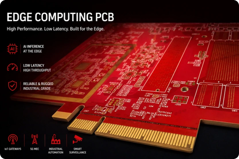
The global edge computing market reached $61.1 billion in 2024 and is projected to exceed $232 billion by 2030, driven by AI inference at the point of data creation, 5G network densification, and industrial IoT deployments that cannot tolerate the 20–100 ms round-trip latency of cloud processing. Edge computing moves intelligence from centralized datacenters to where data originates — inside factory controllers running real-time defect detection, autonomous vehicles making 100 ms driving decisions, smart cameras performing face recognition at 30 fps, and 5G base stations processing user-plane traffic at the tower site.
The Edge Computing PCB faces a design contradiction that doesn't exist in datacenter hardware: it must deliver datacenter-class processing density (NVIDIA Jetson Orin at 275 TOPS, Qualcomm QCS8550 at 48 TOPS) within form factors that survive industrial reality — confined enclosures without fans, temperature swings from -40°C to +85°C, sustained vibration from co-located machinery, and power sources ranging from 12.95W PoE to automotive 12/24V with superimposed load dump transients. Solving this contradiction requires coordinated thermal, signal integrity, and environmental protection engineering that few board designs demand simultaneously.
With over 300 edge computing board programs delivered since 2019 — including carrier boards for NVIDIA Jetson (Nano, Xavier NX, Orin), Qualcomm QCS (QCS6490, QCS8250, QCS8550), and Intel Movidius platforms — HILPCB provides full-cycle PCB fabrication and assembly for edge computing hardware deploying across manufacturing, logistics, healthcare, transportation, and smart city infrastructure worldwide.
Menu Navigation
- The Edge Design Contradiction: Datacenter Power in Industrial Reality
- Signal Integrity for Edge SoC Platforms at DDR5 and PCIe Gen 4
- Fanless Thermal Architecture for Sealed Enclosures
- Multi-Source Power Delivery in Constrained Budgets
- Environmental Hardening for Field Survival
- Prototype-to-Volume Manufacturing for Edge Hardware OEMs
The Edge Design Contradiction: Datacenter Power in Industrial Reality
Traditional server motherboards assume climate-controlled racks with unlimited airflow, clean stable power from redundant UPS, and generous board real estate for routing and thermal management. Edge computing PCBs operate under opposite conditions — sealed die-cast enclosures with zero airflow, power from PoE injectors or automotive batteries with voltage sags and transients, and board dimensions constrained by COM Express (95×125 mm), SMARC (82×50 mm), or custom form factors smaller than a smartphone.A surveillance AI camera on a streetlight in Dubai (55°C ambient, direct sun exposure), a predictive maintenance controller bolted to a CNC machine in Stuttgart (sustained vibration, EMI from motor drives), and a 5G MEC server in a roadside cabinet in Toronto (-35°C winter, 40°C summer with humidity cycling) all share the same board-level engineering challenge. Our design review process addresses these competing constraints through multi-domain co-optimization — thermal, signal integrity, power, and environmental protection engineered as a coordinated system rather than sequential design steps.
Edge PCB Design Differentiators
- Mixed-Signal Density on Compact Boards: Edge SoCs integrate CPU, GPU, NPU, ISP, and I/O controller on a single die — requiring 10–16 layer boards routing DDR4/5 (3200–6400 MT/s), PCIe Gen 4 (16 GT/s), MIPI CSI-2 (2.5 Gbps/lane), USB 3.2 (10 Gbps), GbE, CAN FD, and antenna feeds simultaneously on boards measuring 80×120 mm.
- Thermal Survival Without Active Cooling: Operating at 75°C+ ambient with 15–30W SoC dissipation and zero airflow — the PCB's copper weight, thermal via density, and component placement determine whether the processor runs at full performance or throttles to 60% within 10 minutes of sustained inference workload.
- I/O Protocol Diversity: A single edge board may carry USB 3.2 (90Ω differential), GbE (100Ω differential), CAN FD (120Ω single-ended), RS-485 (120Ω), GPIO (unterminated), PoE power (traces carrying 2A+), and 2.4/5 GHz antenna feeds — each with unique impedance, isolation, and EMI requirements that must coexist within millimeters of each other. The same mix appears on an IoT gateway PCB that bridges field buses to the cloud.
- Compact Form Factor Constraints: COM Express Type 7 (95×125 mm), SMARC (82×50 mm), and custom Jetson carrier formats pack the routing density of a server board into a fraction of the area — requiring HDI PCB construction with 0.1 mm microvias and 3/3 mil trace/space on 10–16 layers.
Signal Integrity for Edge SoC Platforms at DDR5 and PCIe Gen 4
Modern edge processors push data rates where signal integrity becomes the primary yield-limiting factor on compact boards. DDR4 at 3200 MT/s, LPDDR5 at 6400 MT/s, PCIe Gen 4 at 16 GT/s, and MIPI CSI-2 at 4.5 Gbps (for 8K camera input) all demand controlled impedance, matched trace lengths, and low-loss routing — tolerances that compound when squeezed onto a 10-layer board measuring 95×125 mm where every routing channel is contested.Edge Signal Integrity Process
- Pre-Layout Stackup Optimization: Impedance targets (50Ω single-ended, 85Ω/90Ω/100Ω differential depending on interface) simulated across the proposed layer stack — selecting dielectric thickness and copper weight to simultaneously hit DDR (40Ω), PCIe (85Ω), USB (90Ω), and Ethernet (100Ω) targets within ±7% on a single stackup construction.
- Constraint-Driven High-Density Routing: DDR4/5 byte lanes length-matched within ±2 mil, PCIe differential pairs at ±1 mil skew, MIPI CSI lanes routed on inner stripline layers shielded by continuous ground planes — all competing for the same 6 signal layers on a 10-layer high-speed PCB construction.
- Material Selection by Interface Speed: For DDR4 and GbE-only edge boards, high-Tg FR-4 with Dk 4.2 at 1 GHz provides adequate signal integrity at lower cost. For LPDDR5, PCIe Gen 4, or 5G mmWave interfaces, low-loss laminates (Dk 3.4, Df 0.005 at 10 GHz) reduce insertion loss by 30–40% — the material decision directly trades board cost against signal margin.
- Production Impedance Verification: Every production panel includes impedance test coupons measured with TDR — confirming ±7% adherence to design targets across all controlled impedance classes on the board.
Fanless Thermal Architecture for Sealed Enclosures
Edge devices increasingly deploy as fanless sealed units (IP65/IP67) — eliminating fan failure as a reliability concern but making the PCB's thermal architecture the sole path for heat extraction. When an NVIDIA Jetson Orin module dissipates 25W inside a die-cast aluminum housing at 65°C ambient with zero airflow, the thermal design must extract 25W through conduction alone — through the PCB, through the TIM, into the housing, and ultimately to the environment through radiation and natural convection from the enclosure surface.A thermal design with only 5°C margin between steady-state junction temperature and the processor's throttling threshold (typically 100–105°C) will trigger throttling during summer peak loads — reducing inference throughput by 30–40% during the exact conditions (bright sunlight, high temperature) when AI vision systems are most needed.
Thermal Architecture for Sustained Edge Performance
- Dense Thermal Via Arrays: Filled and capped vias (IPC-4761 Type VII) beneath SoC, PMIC, and PoE controller — 0.25 mm diameter at 0.6 mm pitch providing >15 W/cm² thermal conductivity from top-side BGA pad field to bottom-side heatsink contact pad. Via fill (copper for maximum conductivity, conductive epoxy for cost-sensitive designs) and surface planarization to ±10 μm prevent solder wicking during SMT assembly.
- Copper Thermal Plane Distribution: 2–3 inner layers allocated as dedicated thermal planes with 2–3 oz copper — spreading heat laterally from the concentrated SoC die footprint (typically 15×15 mm) to the full board area before conducting through bottom-side thermal pads to the enclosure. Thermal planes designed with minimal splits to avoid thermal resistance barriers.
- Component Thermal Zoning: High-dissipation components (processor module, voltage regulators, PoE controller) physically separated from temperature-sensitive components (MEMS IMU, crystal oscillators, ambient temperature sensors) by ≥20 mm — preventing thermal cross-coupling that degrades sensor accuracy and timing stability.
- IR Thermography Validation Protocol: Every new board design undergoes thermal characterization under worst-case conditions (maximum ambient, maximum processing load, maximum solar loading for outdoor units) — with thermocouple-verified junction temperatures confirming ≥15°C margin below rated throttling threshold.
Multi-Source Power Delivery in Constrained Budgets
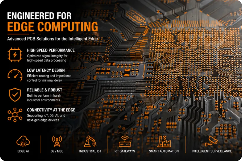
Edge platforms run on diverse, often challenging power sources — PoE Type 3 (25.5W) or Type 4 (71W), 12V barrel jack, automotive 12/24V with load dump transients up to 40V, industrial 24/48V with brown-out conditions, or battery with wide voltage variation. The PCB must accept this input diversity while delivering clean, stable power to processors requiring <5 mV ripple on sub-1V core rails — making power delivery design as critical as signal integrity for edge computing reliability.Power Architecture for Edge Platforms
- Wide-Input Power Front End: Supporting 9–57V input (covering PoE, automotive 12V/24V, industrial 48V) with transient protection meeting ISO 7637-2 (automotive) and IEC 61000-4-5 (industrial surge) — enabling a single PCB design to serve multiple market segments, reducing SKU proliferation and qualification cost for OEMs.
- Multi-Phase Core Regulators: SoCs drawing 10–25A at 0.65–0.85V core voltage require 3–6 phase buck converters with DrMOS stages and inductors placed within 3 mm of SoC power balls — power loops routed with minimal enclosed area on multilayer boards to control switching noise below 10 mV ripple at the processor pad.
- PDN Impedance Engineering: Power distribution network impedance maintained below target impedance (typically 5–15 mΩ from DC through 100 MHz) using distributed decoupling placed by impedance simulation — 4.7 μF bulk capacitors for low-frequency response, 100 nF mid-frequency, and 100 pF high-frequency capacitors positioned by electromagnetic simulation to flatten the impedance curve.
- Light-Load Efficiency for Battery Life: Edge devices idle 80%+ of their operating time (event-triggered inference). Converters with <50 μA quiescent current and pulse-frequency modulation (PFM) mode minimize standby consumption to <200 mW total board power — extending battery life from days to months for remote monitoring applications.
Environmental Hardening for Field Survival
Edge hardware deploys where servers cannot survive — factory floors with cutting fluid mist, outdoor cabinets cycling between -35°C and +55°C daily, agricultural equipment with sustained vibration and dust exposure, and maritime installations with salt spray and 95% humidity. The PCB must operate reliably for 7–10 years under conditions that destroy consumer electronics within weeks.Environmental Protection Engineering
- Extended Temperature Range: Industrial qualification from -40°C to +85°C (operating), -55°C to +125°C (storage) using high-Tg laminates (Tg ≥ 175°C) with solder joints validated through 1,500+ thermal cycles per IPC-9701 across the full operating range — exceeding standard 500-cycle qualification by 3×.
- Vibration and Mechanical Shock: Corner staking adhesive on large passive component arrays (>0805 size), underfill on critical BGA packages (SoC, FPGA, DDR), and board mounting provisions with vibration-damping grommets — validated for IEC 60068-2-6 (sinusoidal vibration, 10–500 Hz, 2g) and IEC 60068-2-27 (mechanical shock, 50g, 11 ms).
- Moisture and Contamination Protection: Conformal coating per IPC-CC-830 with chemistry matched to deployment environment — acrylic for indoor industrial (easy rework), silicone for outdoor installations requiring continuous operation at 95% RH and -40°C to +200°C temperature range, and parylene for medical and defense applications requiring pinhole-free moisture barrier.
- EMI/EMC Compliance Without External Shielding: Filtered I/O with integrated ESD protection, continuous ground planes with <5 mm maximum slot length, and shielded clock routing achieving FCC Part 15 Class B emissions and IEC 61000-6-2 industrial immunity without external shielding enclosures — reducing enclosure cost and simplifying thermal design.
Prototype-to-Volume Manufacturing for Edge Hardware OEMs
Edge computing hardware evolves rapidly — new SoC generations every 12–18 months, expanding sensor suites (LiDAR, mmWave radar, multi-spectral cameras), and market-specific customization (automotive, medical, industrial, defense) drive frequent board revisions. The manufacturing model must support rapid iteration at prototype stage while maintaining quality at 50,000-unit production volumes.Production Scaling for Edge Programs
- Rapid Prototype: 5–50 boards in 5–7 working days with full component sourcing and assembly — enabling hardware validation, thermal characterization, and regulatory pre-testing before production tooling commitment.
- Pilot Production and Certification: 100–500 board runs providing units for environmental qualification (HALT/HASS), regulatory certification (FCC, CE, ISED, VCCI), and customer field trials — with manufacturing process parameters locked after pilot validation.
- Volume Production at Scale: 1,000–50,000+ units per month with automated SMT, in-circuit test, functional test, conformal coating, and final packaging — maintaining consistent quality through SPC-monitored processes and 100% AOI/X-ray inspection.
- Supply Chain Resilience: Approved vendor lists with qualified second sources for all single-sourced components, 8-week buffer stock for long-lead ICs, and proactive end-of-life management — preventing line-down events that delay edge hardware deployments.
Edge Computing PCB FAQ
How do edge computing PCBs manage heat in fanless enclosures?
Edge boards in sealed enclosures rely entirely on conduction for cooling. This is achieved using dense thermal via arrays beneath the processor, dedicated internal copper thermal planes (2-3 oz) for lateral heat spreading, and separating high-power components from temperature-sensitive sensors.
What makes routing on an edge computing PCB so difficult?
Edge PCBs pack datacenter-class capabilities—like DDR5, PCIe Gen 4, and MIPI CSI-2—onto extremely compact form factors like COM Express or SMARC. This requires High Density Interconnect (HDI) construction, microvias, and precise impedance control across multiple high-speed interfaces coexisting in a very confined area.
How do edge PCBs survive harsh industrial environments?
They are engineered for durability using high-Tg FR-4 laminates for thermal stability (-40°C to +85°C), conformal coatings to protect against moisture and contaminants, and underfill/staking to withstand severe mechanical shock and vibration.
Launch your edge computing hardware program — contact our embedded design team →