
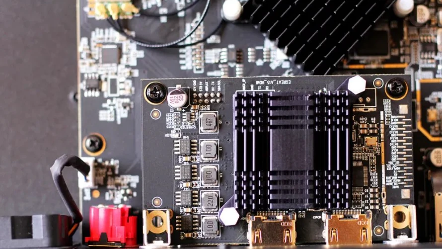

The global electronic warfare market reached $18.3 billion in 2024, with EW systems deployed on virtually every military aircraft and naval vessel across NATO forces. Electronic warfare systems are among the most demanding applications in defense electronics. An EW PCB must receive, analyze, and respond to hostile radar and communication signals across 0.5–40 GHz — often within microseconds. The board's material system, stack-up architecture, shielding design, and fabrication quality directly determine whether the system can detect a threat, classify it, and deploy a countermeasure before the adversary completes a single radar scan.
Unlike narrowband commercial RF boards operating at a single frequency, EW PCBs must maintain controlled impedance and low insertion loss across decades of bandwidth simultaneously. A single board may carry a wideband receiver front-end (2–18 GHz), a DDS for jamming waveforms, high-speed ADCs at 10+ GSPS, FPGA signal processors, and high-power amplifier drivers — all within a ruggedized, thermally managed enclosure.
EW systems are developed and deployed by defense forces across the United States, United Kingdom, Germany, France, Canada, and Australia. HILPCB manufactures EW PCBs on Rogers, PTFE, and Megtron hybrid stack-ups with the impedance control, isolation, and environmental qualification that these programs demand.
HILPCB Manufacturing Capability: We fabricate electronic warfare PCBs on Rogers/PTFE and Megtron hybrid stack-ups with impedance control to ±5% across 2–18 GHz, 16–24 layer constructions, and IPC-6012 Class 3 qualification for EW programs across NATO defense forces.
In This Guide
- Wideband Material Selection and Hybrid Stack-Up Design
- ESM Receiver and Jammer Board Architecture
- Impedance Control Across Decades of Bandwidth
- EMI Hardening and Self-Interference Management
- Thermal Management and Environmental Qualification
- HILPCB Electronic Warfare PCB Manufacturing
Wideband Material Selection and Hybrid Stack-Up Design
EW boards must carry signals from 0.5 GHz through 40 GHz — a frequency range where standard FR-4 dielectric loss makes the board unusable above 6–8 GHz. Material selection is the foundation of every EW PCB design, and hybrid stack-ups combining multiple material types are the standard architecture.At HILPCB, our hybrid stack-up fabrication combines low-loss RF materials with standard digital laminates in a single board — delivering the wideband performance of Rogers/PTFE on signal layers with the mechanical stability and cost efficiency of FR-4 on power and non-critical layers.
Material and Stack-Up Engineering
- RF Signal Layers: Rogers 4003C (Dk 3.38, Df 0.0027 at 10 GHz) or PTFE (Dk 2.2, Df 0.0009) for receiver, synthesizer, and transmit signal paths maintaining insertion loss below 0.15 dB/inch at 18 GHz.
- Digital Processing Layers: Standard high-Tg FR-4 or Megtron 6 for FPGA routing, DDR4 memory, and power distribution — reducing material cost by 40–60% versus all-Rogers construction.
- Hybrid Bonding: Sequential lamination bonding RF and FR-4 materials with compatible prepreg, validated for thermal cycling reliability through 1000+ cycles per IPC-9701 at the -55°C to +85°C military range.
- Layer Count: 16–24 layers with sequential build-up enabling via transitions between RF and digital sections while maintaining impedance continuity through each transition.
ESM Receiver and Jammer Board Architecture
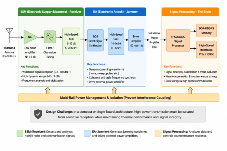
An EW system divides into ESM (receiver), EA (jammer), and signal processing — each with distinct PCB requirements that must coexist on boards sharing the same enclosure or even the same [multilayer](/products/multilayer-pcb/) construction.At HILPCB, our EW board designs address the coexistence challenge of ultra-sensitive receivers and high-power jammers through physical isolation, filtered interconnection, and ground architecture that prevents self-interference.
EW Functional Block Design
- ESM Receiver: Wideband LNA (noise figure <3 dB across 2–18 GHz) with frequency channelizers or digital tuners feeding 8–12 bit ADCs at 5–20 GSPS. The board maintains 50Ω across the entire bandwidth with insertion loss below 0.3 dB/inch.
- EA Jammer: DDS waveform generation with 14–16 bit DACs at 10+ GSPS driving amplifiers delivering 100 mW–1 W to external power amps. Power supply filtering prevents jammer switching noise from coupling into the ESM receiver.
- Signal Processing: FPGA-based threat classification and countermeasure selection on HDI sections with BGA escape routing for 1500+ pin packages.
- Receiver-Jammer Isolation: >80 dB isolation between ESM and EA sections through ground plane partitioning, filtered interconnections, and physical separation with shielding walls soldered to the board surface.
Impedance Control Across Decades of Bandwidth
Commercial RF boards maintain impedance at a single frequency. EW boards must hold 50Ω ±5% from 500 MHz through 18+ GHz simultaneously — a 36:1 frequency ratio where trace geometry, dielectric properties, and via transitions all behave differently at the low and high ends of the band.At HILPCB, our wideband impedance control addresses the frequency-dependent behavior that makes EW fabrication fundamentally different from narrowband RF production.
Wideband Impedance Engineering
- Frequency-Dependent Dk: Dielectric constant varies with frequency — Rogers 4003C shifts from Dk 3.55 at 1 GHz to 3.38 at 10 GHz. We model impedance at multiple frequencies across the band and optimize trace width for best average impedance.
- Surface Roughness: Copper roughness becomes significant above 10 GHz, adding 0.1–0.3 dB/inch of conductor loss. We specify smooth copper foil (HVLP or RTF) on RF signal layers.
- Via Transitions: Every via adds frequency-dependent reflection. Anti-pad optimization, back-drilling (stub <8 mil), and via fence grounding minimize via-induced impedance discontinuity.
- Production Verification: TDR impedance measured on every panel at multiple frequencies, with S-parameter characterization on first articles confirming wideband performance meets simulation.
EMI Hardening and Self-Interference Management
An EW system simultaneously operates highly sensitive receivers and powerful jammers — creating self-interference challenges more severe than any other electronic system. The PCB must prevent the jammer from desensitizing its own receiver while also surviving the electromagnetic environment of a military platform surrounded by radar, communications, and weapons systems.At HILPCB, our EMI hardening approach for EW boards addresses both self-interference management and external electromagnetic survival through coordinated shielding, filtering, and ground architecture.
EMI Management Techniques
- Ground Plane Architecture: Continuous reference planes beneath all signal layers with via-stitched borders creating Faraday-cage isolation between functional sections. Ground plane splits only at defined boundaries with filtered crossings.
- Shield Wall Integration: Soldered shield walls between receiver and jammer sections providing >80 dB isolation. Board layout includes shield wall footprints with adequate ground via spacing (<λ/20 at maximum frequency).
- Power Supply Isolation: Separate voltage regulators for receiver and jammer sections with heavy copper distribution preventing conducted noise coupling through shared power rails.
- MIL-STD-461G Compliance: Conducted and radiated emission/susceptibility testing across the full frequency range, with board-level EMI control designed to meet requirements without relying on external enclosure shielding alone.
Thermal Management and Environmental Qualification
EW systems operate in extreme military environments — from desert heat to arctic cold, on platforms experiencing sustained vibration, shock, and altitude changes. High-power jammer sections dissipating 10–50 W in compact enclosures create thermal management challenges that must be solved at the board level.At HILPCB, our EW thermal and environmental design ensures reliable operation across the full MIL-STD-810H severity range with particular attention to the thermal cycling and vibration conditions of airborne and shipboard EW installations.
Thermal and Environmental Design
- Jammer Section Cooling: Thermal via arrays beneath power amplifier drivers and synthesizer ICs connecting to chassis-mounted heatsinks. High-thermal material options for boards with concentrated heat dissipation.
- Temperature Range: -55°C to +85°C operation on materials validated for thermal cycling reliability. Component derating per MIL-HDBK-217 for 50,000+ hour MTBF at rated temperature.
- Vibration Survival: BGA underfill, component staking, and strain-relieved connectors for platforms experiencing 5–2000 Hz at 5G RMS.
- SMT Assembly with J-STD-001 Class 3 soldering, 100% AOI and X-ray inspection, and 72-hour burn-in at elevated temperature for defense program deliverables.
HILPCB EW and Defense RF Programs
HILPCB fabricates electronic warfare PCBs for defense contractors and EW system integrators across the United States, United Kingdom, Germany, France, Canada, and Australia.
Our capabilities include Rogers/PTFE/Megtron hybrid stack-ups with sequential lamination, wideband impedance control to ±5% across 0.5–18+ GHz with TDR and S-parameter verification, 16–24 layer HDI for FPGA signal processing sections, shield wall integration and ground plane architecture for >80 dB receiver-jammer isolation, heavy copper and high-thermal options for jammer power dissipation, and IPC-6012 Class 3 fabrication with full traceability. From prototype through production, our process delivers the wideband RF performance that EW systems demand.
Electronic Warfare PCB FAQ
Why do electronic warfare PCBs use hybrid stack-ups?
EW systems process ultra-wideband signals (0.5–40 GHz) that standard FR-4 cannot support due to severe dielectric loss. A hybrid stack-up combines high-performance RF materials (like Rogers or PTFE) for the critical signal layers with cost-effective FR-4 for the digital and power planes, balancing performance and manufacturability.
How is self-interference managed between EW receivers and jammers on the same board?
To prevent a high-power jammer from blinding an adjacent sensitive receiver, the PCB employs extreme isolation techniques. This includes partitioned ground planes, soldered shield walls providing >80 dB of isolation, and separate filtered power regulators for each section.
How do you maintain controlled impedance across decades of bandwidth?
Maintaining a flat 50Ω impedance from 500 MHz to 18+ GHz requires modeling frequency-dependent dielectric constant (Dk) variations, using ultra-smooth copper foils (HVLP) to reduce conductor loss at high frequencies, and minimizing via stub reflections through back-drilling.