
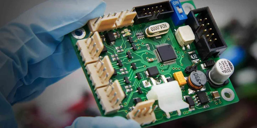
As a power-drive engineer, I know how complex and unforgiving industrial robotics control systems can be. The core is not only precise algorithms, but also the PCB that carries those algorithms and drives real-world motion. From prototype to volume, every step is risky. First Article Inspection (FAI) is no longer a simple manufacturing checkpoint—it’s the engineering foundation that ensures stable operation under high speed, high voltage, and high reliability constraints. It is a full verification pass meant to uncover any hidden defects in design, materials, or process that could trigger field failure.
From a power-drive perspective, this article breaks down First Article Inspection (FAI) for industrial robotics control PCB with focus on IGBT/GaN drive, safety protection, signal sampling, and EMC. We show how FAI validates robustness on first articles—ensuring a smooth transition from Encoder interface board low volume pilot runs to PROFINET control PCB mass production—and ultimately delivering safe, reliable, high-performance robotics control systems.
IGBT/GaN gate drive: verifying Miller suppression and common-mode noise control in FAI
In industrial servo drives, the switching behavior of power devices like IGBT and GaN directly determines efficiency, response speed, and EMC. The gate-drive circuit is the “nervous system” controlling these “muscles”, and its quality must be fully validated during First Article Inspection (FAI).
Quantifying and suppressing the Miller effect
The Miller capacitance (Cgc) is a “natural enemy” of power devices: it creates a Miller plateau during switching, extends switching time, increases loss, and can even cause parasitic turn-on. In FAI, Miller validation is critical.
FAI validation checklist:
- Vge(th) measurement and Miller-plateau analysis: use a high-bandwidth differential probe to measure gate-emitter voltage (Vge). On FAI samples, confirm that during switching transients the Miller-plateau voltage stays well below the device threshold Vge(th). Any induced voltage caused by high dV/dt that stacks onto the plateau can lead to catastrophic shoot-through.
- Gate resistor (Rg) optimization verification: Rg is a trade-off between switching speed and oscillation. In FAI, test gate waveforms under different load conditions (stall, light load, etc.). Verify the chosen Rg suppresses gate ringing while still meeting switching-speed targets—typically by comparing simulation to measured waveforms and confirming margin.
- Negative turn-off and active Miller clamp: for high-speed switching, especially in half-bridge topologies, verify the negative turn-off network or active Miller-clamp function works correctly. Under worst-case dV/dt, confirm the turn-off gate voltage is reliably clamped to 0 V or negative voltage to prevent parasitic turn-on.
Reviewing the drive-supply network and common-mode noise paths
Drive-supply stability and isolation performance are prerequisites for reliable gate drive. In FAI, the power path deserves the same rigor.
FAI review checklist:
- Decoupling and local energy storage: inspect the decoupling capacitors near the driver IC supply pins (often ceramic + tantalum/electrolytic). In full-load switching tests, confirm transient droop stays within the driver IC spec. This is essential for stable drive strength.
- Common-mode current path analysis: high dV/dt creates common-mode current through parasitic capacitance between the power device and heatsink, disturbing the control side. In FAI, use a current probe to measure CM current paths and evaluate whether the isolation supply common-mode capacitance (Cp) is small enough. Also check for unintended CM return paths in layout (e.g., signals crossing an isolation barrier). This is especially important for high-reliability designs such as automotive-grade Encoder interface board.
Passing gate-drive validation is step one for successful Servo motor driver PCB testing, and it lays a solid foundation for the rest of the power-stage verification.
DESAT and short-circuit protection: key safety checkpoints in FAI
Industrial robotics operate in complex environments where motor stall and phase-to-phase faults happen. Fast and reliable short-circuit protection is the lifeline that prevents IGBT/GaN damage and reduces fire risk. Desaturation protection (DESAT) is one of the most common and effective mechanisms, and its performance must be strictly verified in First Article Inspection (FAI). This is a core part of the Dual-channel safety control PCB checklist.
DESAT response time and threshold-voltage tests
DESAT works by monitoring Vce during IGBT conduction. Under normal conduction, Vce is low (saturation). Under short-circuit, current surges and Vce quickly rises out of saturation. The DESAT circuit detects this change and turns off the gate drive immediately.
FAI validation flow:
- Threshold accuracy verification: the DESAT trigger threshold (typically 7–9 V) is set by divider resistors and an internal reference. In FAI, use a precision supply to emulate Vce and measure the real trigger voltage, then compare with the design target. The threshold must be far above normal saturation drop yet sensitive enough to detect a short quickly.
- Response-time measurement: this is the most critical DESAT metric. FAI testing should be performed under controlled short-circuit conditions (e.g., using a low-inductance power resistor to emulate a short). With an oscilloscope, monitor short-circuit current, Vce, and the gate signal to measure total delay from fault onset to the start of turn-off. This typically must be in the microsecond (μs) range; for SiC/GaN, even nanosecond (ns) class may be required. Excess delay means the device can be destroyed before protection acts.
- Blanking-time verification: to avoid false triggers from normal turn-on spikes (due to stray inductance), a short blanking time is typically used. In FAI, confirm it is long enough to ignore turn-on spikes yet short enough to catch real short-circuit events.
Soft turn-off and fault-handling logic review
Fast turn-off alone is not enough. Hard turn-off creates huge di/dt and dangerous overshoot. Modern drivers often include soft turn-off.
FAI review checklist:
- Soft turn-off validation: after DESAT triggers, confirm the driver performs soft turn-off as intended (for example, via a larger gate resistor). Measure Vce overshoot during turn-off and ensure it stays within the device Safe Operating Area (SOA).
- Fault reporting and reset logic: confirm that after a DESAT event, the fault signal (FLT) is latched and reported to the main controller. Also validate reset logic so that the drive cannot be re-enabled before the fault is cleared. This is essential to functional safety under the Dual-channel safety control PCB checklist.
With this level of DESAT validation in FAI, you can be confident that even the harshest fault conditions will be handled without sacrificing an expensive power module—or the system itself.
Type 4: FAI safety-protection reminders
- DESAT response time: turn-off must finish before the device thermal limit under short-circuit current is reached. FAI measurement is the only real standard.
- Over-temperature protection (OTP): verify NTC/PTC sensor placement, thermal coupling, and controller shutdown thresholds to ensure timely protection if cooling fails.
- Under-voltage lockout (UVLO): test UVLO thresholds for both the drive supply and control supply to prevent driving power devices under unstable voltage (linear-region stress and damage risk).
- Fault isolation and reporting: ensure every protection action is correctly detected by the main controller and triggers the predefined safe shutdown procedure—this is the basis of functional safety.
Snubber and clamp networks: RC/TVS performance assessment in FAI
At power-switch turn-off, stray inductance creates severe voltage overshoot and ringing. A snubber (RC/RCD) or clamp circuit is designed to suppress overshoot, clamp voltage within device limits, and improve EMC. First Article Inspection (FAI) is the best time to validate the real effectiveness of these passive networks.
RCD/RC snubber parameter verification
RCD (resistor-capacitor-diode) or RC snubbers are the most common passive solutions. Parameter selection directly impacts suppression and the snubber’s own losses.
FAI validation steps:
- Voltage-overshoot measurement: at maximum DC-bus voltage and full-load current, run switching tests. Use a high-bandwidth probe to measure Vce or Vds precisely. The core FAI task is to confirm peak overshoot stays below the device avalanche breakdown voltage (Vbr) with sufficient safety margin (typically 15–20%).
- Ringing suppression evaluation: observe post-turn-off ringing. A well-designed snubber should damp ringing quickly. In FAI, evaluate ringing amplitude and duration; excessive ringing is a major EMC source and can disturb control signals.
- Power loss and thermal assessment: snubbers dissipate energy. In FAI, run extended tests and use thermal imaging to check snubber resistor temperature rise stays within rating. For high power density Servo motor driver PCB testing, resistor selection must consider resistance value, power rating, and pulse capability.
TVS clamp performance evaluation
Transient Voltage Suppressor (TVS) diodes provide another effective over-voltage protection method. They respond in nanoseconds and clamp voltage to a target level.
FAI evaluation checklist:
- Clamping-voltage consistency: on FAI samples, measure TVS clamping voltage and confirm it matches the datasheet and meets design limits. Clamping voltage varies with current, so test at expected peak stray-current levels.
- Parasitic inductance impact: TVS effectiveness depends heavily on the parasitic inductance of its connection path. In FAI, inspect layout carefully: place TVS as close as possible to the protected device, with short and wide connections. Comparing different layout variants can quantify the impact. For fast-switching GaN devices, this can be make-or-break. Excellent layout is a key success factor for Heavy Copper PCB.
- Energy withstand capability: assess whether the worst-case absorbed energy (e.g., maximum-load turn-off) stays within the TVS Safe Operating Area (SOA)—typically confirmed through combined simulation and measurement.
Whether RC or TVS, FAI validation relies on strict PCB layout review. Power-loop and snubber-loop areas must be minimized to reduce stray inductance at the source. This is a detail HILPCB emphasizes in Turnkey Assembly, ensuring design intent is faithfully realized in the physical build.
Current-sense accuracy: calibrating and validating shunt/Hall solutions in FAI
Accurate current sensing is the foundation for high-performance servo control (e.g., FOC) and reliable over-current protection. Whether using a shunt resistor or a Hall-effect sensor, the sensing chain’s accuracy, bandwidth, and SNR must be fully calibrated and validated during First Article Inspection (FAI).
FAI validation for shunt-resistor sensing
Shunts are favored for high accuracy, low drift, and wide bandwidth—but the challenge is handling common-mode voltage while amplifying tiny differential signals.
FAI validation checklist:
- Gain and offset calibration: inject accurate DC current on FAI samples and measure the entire chain output (shunt → differential amplifier → ADC). Verify gain and offset match expectations. For volume programs such as PROFINET control PCB mass production, define a standardized calibration procedure and lock it down during FAI.
- CMRR testing: in three-phase inverters, shunt common-mode voltage swings violently with switching. In FAI, test real CMRR performance under high-frequency common-mode voltage. A practical method is to compare sampled noise levels at low vs. high DC-bus voltage to qualitatively evaluate suppression.
- Bandwidth and SNR evaluation: inject a sine current with known frequency and amplitude and measure -3 dB bandwidth. With zero current, measure RMS output noise to compute SNR. This is critical for high-dynamic-response Servo motor driver PCB testing.
- PCB layout review: Kelvin connection is the lifeline for shunt sensing. In FAI, use a multimeter or microscope to verify routing strictly follows Kelvin principles to prevent lead resistance and power-loop current from polluting sense accuracy.
FAI validation for Hall-effect sensing
Hall sensors provide natural isolation and simplify the design, but their accuracy, bandwidth, and temp drift are typically worse than shunts.
FAI validation checklist:
- Linearity and hysteresis tests: across the full range, ramp current up and down and plot input-output curves. Check linearity and specifically look for hysteresis (different readings at the same current when increasing vs. decreasing).
- Temperature-drift tests: place FAI samples in a temperature chamber and measure zero and gain drift at different points (e.g., -40°C, 25°C, 125°C). This is essential for wide-temperature applications (e.g., automotive-grade Encoder interface board requirements).
- External magnetic-field immunity: Hall sensors are sensitive to external fields. In FAI, place a magnet nearby or run high current through a nearby wire and evaluate reading stability. Verify the PCB includes effective magnetic shielding measures.
Regardless of approach, the final FAI goal is to ensure the current-sensing system delivers accurate, reliable data across all conditions—providing solid inputs for control and protection decisions.
Type 1: current-sensing approach—FAI spec comparison
| FAI validation item | Shunt-resistor approach | Hall-effect approach |
|---|---|---|
| Accuracy & linearity | High (typically < 0.5%) with excellent linearity. FAI focuses on amplifier gain verification. | Medium (typically 1–2%); may show nonlinearity and hysteresis. FAI must test comprehensively. |
| Bandwidth | Wide (limited by amplifier; up to MHz class). | Limited (typically 100–300 kHz). FAI verifies loop requirements. |
| Temperature drift | Low (mainly depends on resistor material and amplifier). | Higher (zero and gain both drift). FAI must include hot/cold tests. |
| Isolation | None; needs isolation amplifier or isolated ADC. FAI validates isolation performance. | Inherent isolation. |
| Layout sensitivity | Very high; must follow Kelvin connection. FAI requires strict routing review. | Medium; keep distance from high-current paths and external magnetic fields. |
Isolation and creepage/clearance: reliability design review under high dV/dt in FAI
In power-drive systems, isolation protects low-voltage control circuits and operators. It electrically separates the high-voltage power side from the low-voltage control side. With the adoption of wide-bandgap devices like GaN, rapidly changing voltage (high dV/dt) challenges isolation barriers more than ever. First Article Inspection (FAI) must review long-term isolation reliability rigorously.
Physical measurement of creepage distance and clearance
Safety standards (e.g., IEC 61800-5-1) specify minimum Creepage and Clearance requirements for different working voltages.
FAI review checklist:
- Physical dimension measurement: use high-precision calipers or a microscope to measure minimum distances on FAI samples—between HV and LV, between phases, and between live parts and chassis ground. This includes creepage along the PCB surface and clearance through air.
- Slots and V-grooves inspection: if the design uses slots to increase creepage, inspect slot width/depth and edge quality against drawings/process specs. Burrs or residual copper can compromise isolation.
- Coating and potting verification: for boards using conformal coating or potting to enhance insulation, inspect uniformity, thickness, and adhesion. Ensure no bubbles, pinholes, or cracks.
High-voltage testing and CMTI validation
Physical compliance is only step one; electrical validation is the final proof.
FAI validation flow:
- Hi-Pot test: apply AC or DC voltage above rated working voltage (e.g., 2500 Vrms @ 1 minute) and test insulation resistance between HV and LV. No breakdown or arcing should occur. This is the gold standard for basic/reinforced insulation.
- Partial discharge test: for long-term high-voltage operation, partial discharge is a major driver of insulation aging. Using dedicated PD equipment in FAI can detect discharge in micro-voids and evaluate long-term reliability.
- CMTI test: CMTI measures how well isolators (isolated drivers, digital isolators) withstand high dV/dt. In FAI, build a test setup to apply fast common-mode voltage pulses across the barrier (e.g., 50–150 kV/μs) while monitoring for output errors. High CMTI is essential for clean control signals with GaN/SiC. This is especially valuable during Encoder interface board low volume, enabling early discovery.
A first article that passes strict isolation review not only meets compliance—it stays stable and safe in harsh electrical environments. HILPCB’s Prototype Assembly can execute demanding slotting and routing requirements accurately, providing the physical basis for high-reliability isolation designs.
Conclusion: FAI is the required path to excellence and reliability
Industrial robotics control PCB design and manufacturing is a systems engineering effort—combining high-power electronics, precision analog acquisition, high-speed digital communication, and complex functional-safety logic. In such systems, any small oversight can be amplified into performance loss, reliability issues, or even safety incidents.
First Article Inspection (FAI) is the ultimate tool for managing that complexity. It goes beyond a basic “first piece confirmation” and becomes a full, systematic judgment of design theory, component selection, PCB fabrication processes, and assembly quality. From validating Miller suppression in gate drive, to measuring microsecond-level DESAT response; from evaluating snubber clamp performance, to calibrating microvolt-level sensing accuracy; and from reviewing kilovolt-class isolation strength—each FAI step builds the foundation for product success.
For engineers and companies that pursue excellence, a rigorous First Article Inspection (FAI) process is the bridge between Encoder interface board low volume prototypes and PROFINET control PCB mass production. It ensures manufacturability, consistent performance, and long-term reliability. By identifying and resolving issues during FAI, we not only save enormous downstream rework cost—we deliver a serious promise of safety and performance to customers.
Common Questions
Why is FAI critical for industrial robotics control and power boards?
Industrial robotics platforms combine power conversion, motion control, safety logic, and harsh duty cycles in one assembly. FAI confirms that the first hardware build can actually support that complexity before the design is released into broader production.
Why must gate drive, protection, and sensing be validated as one system?
These functions interact directly during switching events, fault response, and closed-loop control. If they are checked separately, timing mismatches or noise issues can remain hidden until the robot is operating under real load.
Why are isolation, creepage, and clearance checks so important in FAI?
Robot controllers often mix high-voltage power stages with low-voltage control electronics and communication circuits. FAI verifies the physical spacing, insulation features, and test results needed to keep operators, equipment, and long-term reliability protected.
How does early FAI help prevent field failures in robotics products?
It uncovers weak solder joints, unstable measurements, protection gaps, and process drift before systems are installed on factory lines. Fixing those issues early reduces commissioning delays, maintenance events, and expensive reliability problems in the field.