
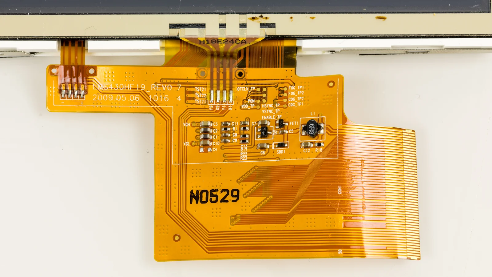
Button plating is a selective copper-plating approach that builds copper in plated holes and their surrounding pad areas while limiting electrolytic copper buildup on flex conductors. It is useful when a design needs reliable layer-to-layer connections but also needs the bend region to remain comparatively thin.
The decision is not simply “button plating is better for flex.” A bend-to-install circuit may work with another plating approach, while a repeatedly moving circuit may benefit from keeping plated copper away from its flexing conductors. In either case, the finished stackup, hole geometry, coverlay, assembly and actual motion determine what must be verified.
For broader process context, see flexible PCB manufacturing. The following design and inspection questions help a designer and fabricator define the order.
What button plating changes
A double-sided flex PCB can use plated-through holes to connect copper layers. The hole barrel needs conductive copper, but the designer may not want the same electrolytic copper buildup along every trace crossing the bend.
In one button-plating sequence, a plating image exposes selected hole and pad regions for copper deposition. The circuit pattern is then imaged and etched in a subsequent operation. Process details vary by fabricator, so “button plated” should be treated as a request for a defined copper distribution, not as a complete manufacturing specification. The Flexible Circuit Technologies design guide describes pads-only, selective and button plating as terms for plating copper in through-holes and on pads. This terminology does not establish a particular supplier's process or capability.
The term pads-only plating is often used for the same general idea. However, a buyer should still clarify exactly which pads are included. A hole surrounded by a plated annulus is different from an isolated surface-mount pad that the designer also wants reinforced. Do not assume every exposed pad receives the same copper buildup.
Button plating is also distinct from the surface finish. Copper plating builds the conductive structure; a specified finish protects or prepares exposed connection areas for assembly or contact. The finish, its application areas and its compatibility with assembly remain separate decisions.
Where the copper is—and is not
For a button-plated design, describe the expected finished construction by location:
- Hole barrel: Plated copper forms the intended interconnection between layers.
- Hole land or annulus: A localized plated area surrounds the hole, subject to the agreed design and manufacturing tolerances.
- Bend conductors: These retain the intended conductor copper without the same nominal electrolytic buildup applied to the buttons. Thin process-related deposits or other variations should not be assumed absent.
- Other pads: Their copper buildup depends on the agreed plating image and process.
- Exposed connection surfaces: These receive the specified finish where applicable; finish thickness is not the same requirement as copper barrel thickness.
A drawing that only says “thin copper in flex area” leaves too much open. Define the bend area and state the required copper condition there, including any permitted exceptions or measurement approach.
Choosing a plating approach
The following matrix is a starting point for a technical discussion, not a claim that one process will meet a particular design or standard.
| Design situation | Approach to investigate | Main reason | Question to resolve |
|---|---|---|---|
| Double-sided circuit with repeated bending | Button or pads-only plating | Localizes heavier electrolytic copper near interconnects rather than intentionally building it across bend traces | Can holes, pads and plating transitions be kept outside the moving zone? |
| Flex bent primarily during installation | Compare button plating with broader copper plating | The motion requirement may be less demanding, but the finished stackup still matters | Does the complete construction fit the available bend and installation method? |
| Current-carrying traces through a bend | Compare copper and trace geometry options | Reducing copper buildup can reduce conductor cross-section | Can the finished bend conductor, including its actual copper thickness and any process deposits, carry the required current at an acceptable temperature? |
| Dense pads or small holes near a bend | Review geometry with the fabricator before choosing | Registration, annular ring and plating-image constraints may compete for space | Is there room for a robust pad and an adequate transition away from the bend? |
| Isolated surface pads requiring reinforcement | Request an explicit local-plating review | Hole-button plating does not automatically define treatment of every pad | Which pads are plated, and how will local thickness be controlled? |
Button plating can add imaging and process-control work. Its effect on cost and lead time depends on the design, order quantity and supplier’s process; request a quote rather than assuming a fixed premium.
If repeated motion is central to the application, also review dynamic flex PCB design. A plating choice does not replace motion-specific testing.
Design the bend region as a system
Start with the actual motion
Mark the flexing region on the fabrication drawing and identify whether bending occurs during installation, during normal use, or both. For repeated motion, describe the bend path, direction, minimum installed radius, travel, speed, expected cycles and any twisting or off-axis movement.
Keep plated holes, component pads and local copper-thickness transitions outside the active bend where practical. A localized thick or stiff area can change how a nearby section bends; moving a via just beyond a nominal bend line is not enough if the real motion reaches it.
The designer remains responsible for defining the motion and product environment. The fabricator can review manufacturability against that information, but a board quotation alone does not establish that the finished product will survive its duty cycle.
Specify copper by location, not just nominal foil weight
Base foil selection and finished copper are related but different. A useful drawing distinguishes:
- The starting foil type and nominal thickness for each copper layer.
- The desired finished conductor copper condition in the bend.
- The required barrel and pad plating, with applicable acceptance criteria.
- Any locally plated pads outside the bend.
- Surface finish type and locations.
The finished conductor is affected by the manufacturing sequence, including copper deposition and etching. A nominal starting foil value is therefore not automatically a finished minimum trace thickness.
Rolled-annealed copper is often considered for demanding dynamic flex applications, but foil selection alone does not prove fatigue life. A NASA lessons-learned case discusses foil orientation, copper position relative to the neutral bending axis and overlapping conductors in a particular flex-harness failure. Its observations are not a universal life prediction. Ask the fabricator how the specified foil direction will be related to the circuit and panel.
For material background, see PCB copper foil, copper-clad laminate and reading material data sheets for PCB stackups.
Plan trace geometry and transitions
Route through the bend with geometry suited to the mechanical path. Avoid unnecessary abrupt width changes, corners and local features in the most highly flexed area. Consider trace arrangement across layers: stacked conductors and copper shapes can affect local stiffness, while changes to return paths can affect electrical performance.
A wider trace can recover some electrical cross-section when less copper is plated onto it, but width, spacing and routing density must still be manufacturable. A shield or ground pattern is likewise an electrical and mechanical choice: an open pattern may alter flexibility, but it can also change shielding and return-current behavior. Validate both functions rather than selecting a pattern for bendability alone.
Coordinate coverlay and stiffeners
Coverlay openings must provide access to pads without leaving critical features poorly supported. Registration tolerance, pad size and any anchoring features need to be reviewed together. Stiffeners can support connectors and assembly areas, but their edges and termination points also define where the flex can bend.
Document the intended stiffener outline, thickness, location, adhesive and any allowed overlap. Confirm the full stackup in the transition—not only the nominal thickness of the free-flex portion.
A hypothetical copper trade-off
Consider a hypothetical two-layer flex circuit with one conductor crossing a moving bend and a plated through-hole in a supported end region. The designer wants to compare a button-plated bend conductor with an illustrative conductor that receives additional copper.
Assume, solely for an early cross-section comparison:
- Both conductors are 0.20 mm wide.
- The finished bend conductor in the button-plated option is modeled as 12 µm thick.
- The comparison conductor is modeled as 30 µm thick, after an illustrative 18 µm buildup.
- Both are treated as rectangular, ignoring etch profile, process deposits and thickness variation.
| Hypothetical conductor | Simple cross-section calculation | Result |
|---|---|---|
| Button-plated bend area | 0.20 mm × 0.012 mm | 0.0024 mm² |
| Comparison with added copper | 0.20 mm × 0.030 mm | 0.0060 mm² |
Under these simplifying assumptions, the second conductor has 2.5 times the copper cross-sectional area. If material and length were otherwise identical, the smaller cross-section would have higher DC resistance. This is not a current rating, temperature-rise prediction or fatigue-life calculation.
To recover the same idealized cross-section at 12 µm thickness, the designer might examine a 0.50 mm-wide bend trace: 0.50 mm × 0.012 mm = 0.0060 mm². That change consumes routing space and may affect the stackup and electrical behavior. It also does not establish that the circuit will withstand the intended motion.
The next step is to provide the actual current, temperature limit, geometry and motion to the responsible engineering team, then ask the fabricator which finished copper ranges and inspection methods it can quote. Build and test representative hardware before treating either option as qualified.
What to inspect—and what each test can prove
A useful inspection plan separates visible features, hidden construction and application behavior.
| Check | What it can address | Important limitation |
|---|---|---|
| Fabrication-data and drawing review | Bend-zone definition, plating locations, layer connections and stated requirements | A review identifies questions; it does not demonstrate finished-board performance |
| Visual inspection | Accessible pad condition, coverlay registration and visible damage or anomalies | It cannot establish the condition of the entire hole barrel or predict flex life |
| Electrical continuity and isolation | Opens and shorts covered by the agreed net test | A passing room-condition test does not prove fatigue resistance |
| Microsection of agreed coupons or specimens | Local barrel plating, interfaces and internal features at the sectioned locations | Destructive and sampling-based; the result does not inspect every production hole |
| Finished copper verification | Thickness or other agreed attributes at defined locations | Method and location matter; a pad measurement is not automatically a bend-trace measurement |
| Flex or assembly test | Performance under the specified fixture, motion and conditions | Results apply to the tested configuration and do not automatically qualify every installation |
Specify which checks are included in the supplier’s quote, sampling plan, deliverables and disposition of failures. Ask whether coupons represent the relevant hole sizes and construction, and where barrel measurements will be taken. If a critical bend-trace copper requirement cannot be measured directly on delivered boards, agree on a practical verification method before release.
IPC-A-600, Acceptability of Printed Boards, describes externally and internally observable conditions; some internal features require microsectioning for evaluation. IPC-6013, Qualification and Performance Specification for Flexible/Rigid-Flexible Printed Boards, addresses flexible-board qualification and performance. Identify the applicable revisions, class, exceptions and order of precedence in the procurement documents; naming a standard alone is not evidence of acceptance.
Separate lot inspection from product qualification
A fabrication lot can pass its agreed inspection and electrical test while the assembled product still fails its intended motion. Product qualification should address the actual assembly, attachment points, bend path, environment and failure criteria.
A material-oriented flex test can inform an assessment, but its specimen and setup are not automatically representative of a finished product’s motion. Select or develop an application-representative test plan and define who runs it, how continuity is monitored and what constitutes failure.
RFQ checklist for button-plated flex
Before requesting a quote or discussing the design, prepare:
- Fabrication data: Copper layers, drill files, outline, netlist, coverlay, finish openings, stiffeners and drawing revision.
- Flex zones: Clearly marked active bend and transition areas, including prohibited holes, pads or local copper buildup where required.
- Motion: Installation bends, operating motion, minimum radius, travel, cycle target, twist and environmental conditions.
- Stackup: Base materials, adhesive and coverlay, foil type and orientation, nominal thicknesses and acceptable alternatives.
- Plating map: Which holes and pads receive selective copper plating; treatment of isolated pads; and the desired copper condition on bend conductors.
- Hole requirements: Finished hole sizes, tolerances, annular-ring requirements and any required barrel-plating criteria.
- Electrical needs: Current, temperature-rise constraints, impedance or return-path requirements, and the intended surface finish.
- Standards and acceptance: Applicable document revisions, product class, drawing precedence, exceptions and customer-specific criteria.
- Quoted verification: Electrical test, visual inspection, coupons, microsections, sampling, reports and any additional testing.
- Qualification ownership: Who designs the product-level test, supplies fixtures and assemblies, evaluates results and approves release.
Ask the supplier to identify any proposed substitutions or process changes before manufacturing. For related product information, see flex PCB manufacturing and PCB products. Confirm whether the proposed selective-plating construction is available for the specific order.
Is button plating the same as pads-only plating?
The terms are often used for the same selective-plating concept. Still, specify which holes and pads must receive copper and what copper condition is required in the bend region.
Does button plating remove all copper from the bend?
No. The bend still contains the copper conductors needed for the circuit. The objective is generally to avoid the same intentional electrolytic copper buildup used at selected holes and pads.
Can a button-plated flex PCB be used for repeated motion?
It can be considered for repeated motion, but the plating method alone does not establish flex life. The motion, complete stackup, trace geometry, assembly and application-specific test results matter.
How is a button-plated hole inspected?
Visual inspection can assess accessible features; a microsection of an agreed specimen can reveal barrel and interface conditions at the sectioned location. The drawing and quote should define sampling, measurements and acceptance criteria.
Does a passing electrical test qualify the finished product?
No. It shows that the tested connections and isolation met the agreed electrical test conditions. Product qualification may also require representative assembly, environmental and flex testing.