
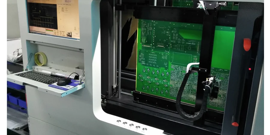
With the rapid growth of AI and high-performance computing (HPC), chip design is accelerating into the Chiplet era and 2.5D/3D heterogeneous integration. AI accelerators, GPUs, and specialized SoCs are scaling power and throughput exponentially—pushing IC Substrate and interconnect PCB requirements to the limit. In this context, ensuring that every micron-scale trace and every microvia connection is electrically flawless becomes a decisive factor for final system performance and reliability. Flying probe test is a high-precision, highly flexible electrical test method—and a core quality gate for these challenges.
As an engineer focused on power integrity, I know how unforgiving AI chips are to PDN defects: massive transient currents, ultra-low impedance paths, and stable voltage delivery. Even small manufacturing issues—opens, shorts, or impedance discontinuities—can trigger catastrophic failures. Traditional test methods struggle with AI substrates featuring <20 μm line/space and 20+ layer complexity. That’s why understanding and using Flying probe test effectively is foundational for seamless design-to-manufacturing handoff and reliable delivery of high-performance AI hardware. Leading manufacturers such as Highleap PCB Factory (HILPCB) deploy advanced flying probe systems to provide reliability assurance from prototype to volume for complex AI substrate designs.
Why is Flying Probe Test foundational for AI substrate manufacturing?
Before diving into applications, it’s important to understand why Flying probe test is indispensable in AI substrate manufacturing. Unlike a traditional Bed-of-Nails test, which requires an expensive dedicated fixture for each PCB design, a flying probe system uses 2–8 (or more) independently moving probes controlled by software to contact test points (pads, vias, component leads) and perform electrical measurements.
This fixtureless approach provides three core advantages that match AI substrate production perfectly:
Unmatched flexibility and turnaround speed: AI chip substrates iterate fast and change frequently. Flying probe test eliminates weeks of fixture lead time. CAD data can be converted to a test program and started within hours. This dramatically shortens NPI cycles—especially in prototype validation and low-to-mid volume builds—while improving cost efficiency.
High precision and high coverage: AI substrate pad pitch is now in the micron range, where bed-of-nails pinning becomes impractical. Flying probes can accurately land on test points as small as ~35 μm, enabling 100% net coverage and detecting tiny opens, shorts, R/L/C deviations, and even some component polarity/orientation mistakes. This precision is critical for high-density interconnect reliability.
Adaptability to ultra-dense designs: Whether CoWoS, InFO, or EMIB, advanced packaging substrates and interposers have extreme routing density. Flying probe test can access dense regions without fixture constraints, enabling comprehensive validation of critical signal paths.
For AI substrates, a minor short can scrap an entire high-value package. Catching all electrical defects at the bare-board stage via Flying probe test is a fundamental lever for yield and cost control.
How does Flying probe test ensure RDL fan-out substrate manufacturing quality?
RDL (Redistribution Layer) is a core technology in advanced fan-out packaging. It redistributes I/O on the die surface via fine metal routing to a larger area to match BGA arrays. RDL fan-out substrate manufacturing involves multiple lithography, plating, and etch steps—highly complex and prone to defects.
Flying probe test plays a key role in ensuring RDL fan-out substrate quality:
Micro-open and micro-short detection: RDL line/space is often 2–10 μm. Minor particle contamination or process drift can cause opens or shorts. Flying probe test uses high-precision Kelvin (4-wire) measurement to detect these defects at the milliohm (mΩ) level—beyond what many conventional methods can reliably achieve.
Interlayer connection reliability validation: Multi-layer RDL structures rely on microvias for layer-to-layer connectivity. Plating quality directly impacts signal and power delivery. Flying probe can measure end-to-end path resistance from top pad to bottom pad, identifying failures or high-resistance connections due to poor plating or misregistration.
Integrity confirmation for low-loss materials: AI high-frequency signaling increasingly uses low-loss RDL fan-out substrate materials such as ABF (Ajinomoto Build-up Film). Even when the base material is excellent, process defects can ruin low-loss behavior. By validating continuity and isolation, flying probe test indirectly confirms the material and build process preserve designed electrical performance. HILPCB combines advanced material know-how with a strict Flying probe test flow to protect RDL fan-out substrate performance.
HILPCB advanced IC substrate manufacturing capability matrix
| Technical parameter | HILPCB capability | Value for AI chips |
|---|---|---|
| Maximum layer count | 56 layers | Supports complex PDN design and high-density signal routing |
| Minimum line/space | 15μm / 15μm | Enables high-density interconnect between Chiplet and HBM |
| Minimum mechanical drill | 0.1mm | Dense via arrays to optimize signal paths |
| Impedance control tolerance | ±5% | Protects SI for PCIe 6.0/CXL and other high-speed links |
| Supported materials | ABF, Megtron 6/7/8, Rogers, Teflon | Meets low-loss and thermal demands across application scenarios |
Choosing HILPCB as your AI substrate/interconnect manufacturing partner means choosing industry-leading precision and process control. Contact us for detailed technical specs.
What is the role of flying probe test in HBM3 interposer PCB impedance control?
HBM is a standard building block for modern AI accelerators. With HBM3/3e pushing per-stack throughput beyond 1 TB/s, impedance consistency along the signal path becomes non-negotiable. Any impedance discontinuity can cause reflections and distortion, driving bit errors. HBM3 interposer PCB impedance control is therefore a core challenge for stable HBM channels.
By integrating TDR capability, Flying probe test systems can directly measure characteristic impedance on selected transmission lines:
- A probe injects a fast-rise step pulse into the trace.
- A high-speed scope monitors the voltage waveform at the injection point.
- If the trace impedance deviates from the target (e.g., 50 Ω), part of the energy reflects back and changes the waveform.
- From reflection amplitude and timing, the system computes impedance along the path and pinpoints discontinuities.
For HBM3 interposers, flying-probe TDR enables:
- Per-line verification: Measure thousands of HBM channels line-by-line and ensure impedance stays within spec (e.g., ±5%).
- Defect localization: Identify where line width, dielectric thickness, or reference-plane distance drifted during manufacturing—direct data for process optimization.
- Pair consistency: Confirm impedance matching inside differential pairs to reduce common-mode noise and preserve signal quality.
Strict HBM3 interposer PCB impedance control via flying probe testing filters out out-of-spec boards before they reach costly downstream die attach and packaging steps. For demanding high-speed PCB designs, this kind of in-process control is essential.
How does EMIB interconnect board impedance control benefit from flying probe test?
EMIB (Embedded Multi-die Interconnect Bridge) is Intel’s 2.5D packaging technology that embeds a small high-density silicon bridge inside the substrate to connect Chiplets at high bandwidth. Compared to full-size silicon interposers, EMIB can reduce cost and improve design flexibility—but it introduces unique test challenges: how do we ensure robust connectivity between organic substrate routing and a tiny silicon bridge interface?
The difficulty in EMIB interconnect board impedance control is the ultra-dense, complex transition region. Flying probe test delivers unique value here:
- Precise access to Micro-bump structures: EMIB uses Micro-bumps to connect substrate to the silicon bridge. Fine probes can contact the corresponding pad region on the substrate and validate the electrical path up to the interface.
- Local impedance behavior analysis: TDR measurement can reveal impedance changes as signals enter the EMIB transition region—helping catch mismatch driven by fabrication drift or lamination/material issues.
- Design-rule verification: EMIB routing rules are strict (angles, via placement, keepouts). Flying probe test validates continuity and isolation to catch unintended opens/shorts caused by manufacturing variation.
Highleap PCB Factory (HILPCB) has extensive experience building dense IC Substrate PCB. We understand the manufacturing constraints of advanced packaging and use Flying probe test and other inspection methods to ensure every delivered substrate meets stringent electrical requirements.
Flying Probe Test vs. Bed-of-Nails in AI substrate applications
| Attribute | Flying Probe Test | Bed-of-Nails Test |
|---|---|---|
| Upfront cost (NRE) | Very low (no fixture) | High (custom fixture) |
| Best-fit volume | Prototype, low-volume, high-mix | High-volume, low-mix |
| Program lead time | Short (hours) | Long (days to weeks) |
| Test pad pitch | Down to 35μm | Typically > 400μm |
| Coverage | 100% net coverage | Limited by fixture design |
| Per-board test speed | Slower (serial) | Very fast (parallel) |
| Design change agility | Very high (software update only) | Low (new fixture required) |
How does flying probe test detect potential issues in PI design?
As a PI engineer, my top concern is whether the AI chip receives stable, clean power. During massively parallel compute bursts, current can jump from near 0 A to hundreds of amps within nanoseconds (ns). This di/dt demands an extremely low-impedance PDN.
Flying probe test is also essential for PDN integrity:
Low-resistance path verification: With high-precision 4-wire measurement, flying probe test validates DC resistance from VRM regions to chip BGA power/ground pads. Any high-resistance bottleneck from poor via plating, insufficient copper thickness, or constricted connections can cause IR Drop under transient load—hurting performance or triggering resets.
Plane-to-plane short detection: AI substrates often exceed 20 layers with interleaved power and ground planes. Minor metal debris or misregistration can short large copper planes—fatal defects. Flying probe test reliably detects low-resistance connections between independent nets, isolating defects early.
Decoupling capacitor pad integrity checks: AI substrates deploy hundreds to thousands of decaps. Flying probe test confirms pads are not shorted to power/ground and are not open—providing a solid base for downstream SMT assembly. A well-designed low-loss RDL fan-out substrate also requires robust PDN design, and flying probe test helps validate it.
Why is flying probe test so cost-effective in prototypes and low-volume builds?
AI chips and substrates go through continuous iteration. Early in development, teams need a handful to dozens of prototypes for functional validation and tuning. In this scenario, Flying probe test shines:
Zero NRE: A bed-of-nails fixture can cost thousands to tens of thousands of dollars—unjustifiable for small prototype quantities. Flying probe test eliminates this cost, reducing prototype expenses significantly.
Fast response to design changes: Layout revisions are routine. With bed-of-nails testing, even minor changes can require a new fixture. With Flying probe test, updated CAD data can refresh the program within hours—keeping pace with design iterations.
A diagnostic and debug tool: When prototypes fail, flying probe test provides more than pass/fail—it can pinpoint faults, e.g., “Net A and Net B shorted at (X, Y), R=0.5 Ω.” This accelerates root-cause analysis and design improvement.
HILPCB’s prototype assembly service deeply integrates Flying probe test. We deliver fast, reliable prototypes with comprehensive electrical verification—helping customers accelerate time-to-market. This flexibility and economics make flying probe testing essential for both AI hardware startups and large enterprise R&D teams.
⚠ Key DFT tips for AI substrates
- Reserve test pads: Add test pads (≥100μm diameter) on key nets, especially near BGA pads that are hard to probe directly.
- Test pad spacing: Keep enough distance between adjacent pads (recommended >0.3mm) to prevent probe mis-contact.
- Avoid solder mask coverage: Test pads must be exposed; do not cover them with solder mask.
- Provide accurate CAD data: Provide an IPC-D-356 netlist—standard input for flying probe programming.
- Flag high-voltage nets: Clearly mark high-voltage nets so the tester can apply safe isolation measures.
Good DFT practice significantly improves Flying probe test efficiency and accuracy. Facing design challenges? HILPCB engineers can provide a free consultation.
What are the future trends for flying probe test, and how will they impact 3D packaging?
As semiconductors move toward 3D-IC and more advanced heterogeneous integration, test requirements continue to evolve—and Flying probe test keeps innovating:
- Higher precision and smaller probes: To test finer routing and Micro-bumps in next-generation packages, probe size will shrink and placement precision will approach sub-micron levels.
- Higher throughput: More probes, optimized motion planning, and parallel test architectures will dramatically increase throughput while keeping fixtureless flexibility—making flying probe more competitive for low-to-mid volume production.
- Multi-function integration: Future systems will integrate AOI, thermal imaging, and high-frequency RF measurement alongside electrical test—enabling one-stop board-level quality evaluation.
- Testing 3D structures: For TSV-stacked 3D-IC, direct probing of internal interconnects is extremely difficult. Flying probe test is exploring combined approaches with techniques such as boundary scan JTAG—inferring internal connectivity health via peripheral I/O response.
In RDL fan-out substrate manufacturing and other advanced substrate builds, the pursuit of quality never stops. Flying probe test is a critical firewall—and its value will keep growing. Choosing a partner like HILPCB that continually invests in advanced test equipment is key to keeping your advanced AI products competitive.
Conclusion: using Flying probe test to protect the interconnect core of the AI era
In the precise and complex world of AI chip interconnect and IC substrate PCB, performance gains come with manufacturing risk. From accurate HBM3 interposer PCB impedance control, to robust EMIB interconnect board impedance control, to reliable low-loss RDL fan-out substrate builds—every step depends on strict quality control. With its fixtureless flexibility, high precision, and dense-design accessibility, Flying probe test is an indispensable guardian across this ecosystem.
It’s not only a tool to catch basic opens and shorts—it’s also a key method to validate SI, PI, and reliability of advanced packaging structures. For AI hardware teams aiming for fast iteration and peak performance, Flying probe test is the foundation for shorter development cycles, lower risk, and successful products.
As your trusted manufacturing partner, Highleap PCB Factory (HILPCB) embeds advanced Flying probe test deeply into our production flow to deliver the highest-quality IC substrates and interconnect solutions for global AI and HPC customers. We understand your design challenges—and we can turn them into reliable, high-performance hardware.
Common Questions
Why is flying probe test so valuable for AI chip interconnect and substrate boards?
Because these products often have dense routing, fine pitch structures, and frequent design changes during development. Flying probe testing provides high coverage without requiring a dedicated fixture, which makes it especially useful when flexibility and precision both matter.
Why does flying probe test matter for signal integrity and power integrity validation?
It does more than find opens and shorts. On advanced interconnect boards, it also helps teams confirm resistance, capacitance, and continuity behavior on critical nets so early electrical risks can be identified before assembly or system integration.
Why is DFT planning important for flying probe test on advanced packaging boards?
Even though flying probe testing is fixtureless, it still depends on accessible pads, safe probe locations, and accurate CAD/netlist data. Good DFT planning makes the test faster, safer, and more reliable on dense AI hardware.
Why will flying probe test remain relevant as packaging moves toward 3D integration?
As packaging gets denser and more complex, direct physical access becomes harder, not easier. Flying probe systems are evolving with smaller probes, better accuracy, and stronger integration with other inspection methods, so they remain a practical frontline tool for advanced builds.