
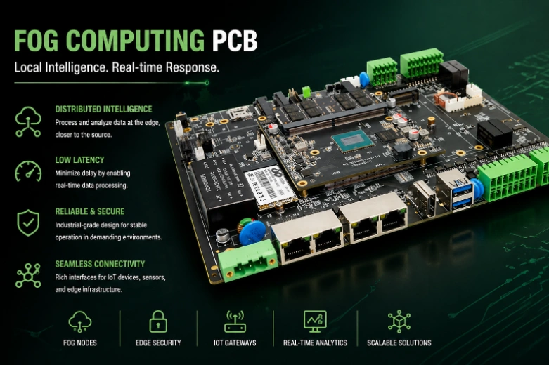
The global fog computing market is growing at 55.6% CAGR, projected to reach $982 million by 2028 as smart city infrastructure, utility grid modernization, and industrial IoT deployments expand across five continents. Fog computing places intelligence between cloud data centers and endpoint sensors — processing, filtering, aggregating, and acting on data at intermediate network nodes rather than forwarding raw sensor streams to the cloud. A fog node doesn't just relay data — it runs local analytics (anomaly detection on vibration signatures, pattern recognition on power consumption profiles), caches results for cloud-disconnected operation, enforces security policies, and manages dozens to hundreds of endpoint devices through multiple wireless and wired protocols simultaneously.
What makes a fog computing PCB architecturally distinct from both edge devices and cloud servers is its role as a multi-protocol aggregation point. A single fog gateway may simultaneously communicate through Ethernet (to upstream cloud), Wi-Fi 6 (to local devices), BLE 5.3 (to asset trackers), LoRaWAN (to remote sensors at 10+ km range), LTE/5G cellular (as WAN backup), RS-485 Modbus (to industrial PLCs), and CAN FD (to vehicle or machinery buses) — each protocol with distinct impedance, EMC isolation, and regulatory certification requirements, all sharing a single PCB.
HILPCB manufactures fog computing PCBs for OEMs deploying smart metering infrastructure across Europe, traffic management systems in the United Kingdom, agricultural IoT networks in Australia, and industrial fog platforms across North America and Asia-Pacific.
Menu Navigation
- Fog Node Architecture: The Aggregation Challenge
- Multi-Protocol RF Coexistence on a Single Board
- Data Resilience: Storage Under Power Instability
- Hardware Security for Connected Infrastructure
- Environmental Durability Across Climate Zones
- Fleet Economics: Cost-Optimized Manufacturing at 5,000–10,000 Units
Fog Node Architecture: The Aggregation Challenge
A fog node occupies an architectural position that creates a unique combination of PCB requirements not found in any other computing category. It needs moderate compute (ARM Cortex-A78 or mid-range x86 such as Intel Atom or AMD Ryzen Embedded) — but dominant I/O throughput. It aggregates data from 50–200 simultaneous sensor connections across 4–7 different communication protocols. It stores data locally for days or weeks when cloud connectivity drops. And it runs continuously for 5–10 years in telecommunications cabinets, factory control panels, or outdoor enclosures — environments where mean time between human visits may be months.This combination — moderate compute, extreme I/O diversity, always-on reliability, and fleet economics requiring low per-unit cost — drives PCB design decisions fundamentally different from either edge computing (high compute, limited I/O) or cloud computing (extreme compute, homogeneous networking).
Core Fog Node PCB Design Trade-offs
- I/O-Dominated Board Architecture: Unlike compute-focused boards where the processor dominates board area and routing complexity, fog node boards dedicate 60–70% of board area to I/O interfaces, antenna systems, isolation barriers, and connector zones — the processor and memory occupy a compact central zone with relatively straightforward routing.
- Always-On Reliability at Fleet Cost: Fog nodes are infrastructure — expected to operate 24/7/365 for 5–10 years without maintenance visits. But fleet deployments of 5,000–10,000 units make per-board cost critical. This creates a design tension: achieving server-class reliability (50,000+ hour MTBF) at IoT gateway price points ($80–$200 per board) through smart material selection and component derating rather than over-engineering.
- Protocol Coexistence Without External Shielding: Supporting 4–7 simultaneous RF and wired protocols without the metal shield cans that add $3–$8 per board — coexistence achieved through PCB layout techniques (ground fencing, strategic antenna placement, filtered power distribution) rather than mechanical shielding.
Multi-Protocol RF Coexistence on a Single Board
The defining technical challenge of fog computing PCB design is routing and isolating multiple communication protocols on a single board without mutual interference — while meeting carrier certification requirements (PTCRB for cellular, Wi-Fi Alliance for Wi-Fi, LoRa Alliance for LoRaWAN) that test each protocol independently and in combination.A typical fog gateway simultaneously operates Wi-Fi 6 (2.4 and 5 GHz), Bluetooth 5.3 (2.4 GHz — sharing band with Wi-Fi), LoRaWAN (sub-GHz: 868 MHz Europe, 915 MHz Americas, 923 MHz Asia), cellular LTE/5G (700 MHz–3.5 GHz), RS-485 Modbus (differential pair at up to 10 Mbps), and CAN FD (differential pair at 5 Mbps). The 2.4 GHz band is particularly challenging because Wi-Fi and BLE share the same frequency range and must coexist without desensitization.
RF and Protocol Isolation Techniques
- Antenna System Design: Wi-Fi, BLE, and LoRa feed points separated by ≥λ/4 at lowest shared frequency (≥30 mm at 2.4 GHz) with ground plane fencing (via fence at λ/20 spacing) between RF sections. Antenna traces routed on dedicated high-frequency PCB layers with Dk-matched dielectric (±5% Dk tolerance) for consistent antenna impedance matching across production lots — critical for passing PTCRB/GCF carrier certification without per-unit tuning.
- Industrial Protocol Galvanic Isolation: RS-485 and CAN FD interfaces with 2.5 kV galvanic isolation per IEC 61000-4-5 using digital isolator ICs with >100 dB CMTI (common-mode transient immunity). Isolation barriers designed with ≥6 mm creepage distance (reinforced insulation rating) with isolated-side power through dedicated isolated DC-DC converters — protecting the fog node from ground potential differences between connected industrial equipment.
- PoE Power Extraction: Multi-port GbE with IEEE 802.3bt Type 4 power extraction (up to 71W) on heavy copper power planes rated for sustained 1.5A per pair — trace routing following IEEE 802.3 power delivery specifications with proper thermal derating for enclosed installations.
- Cellular Modem Integration: Impedance-controlled 50Ω coaxial-to-PCB transitions with <0.3 dB insertion loss to 6 GHz and antenna tuning networks accommodating global frequency bands (Band 1–85) — layout designed for Red Directive/FCC Part 22&24 certification compliance with margin.
Data Resilience: Storage Under Power Instability
Fog nodes cache data locally when cloud connectivity drops — a defining capability that distinguishes fog computing from pure edge processing. A utility fog node monitoring 500 smart meters must continue recording consumption data during a 72-hour cloud outage, storing up to 200 MB of time-series data locally and synchronizing when connectivity restores. Data loss during this period isn't just an inconvenience — for utility billing, it creates revenue leakage and regulatory non-compliance.The PCB storage architecture must handle this critical data caching function under the power instability conditions common in field installations — unexpected power cuts, voltage brown-outs, and lightning-induced transients that can corrupt filesystems and destroy flash storage blocks.
Storage Design for Field Data Integrity
- Industrial-Grade Storage Interface: eMMC (50Ω single-ended HS400 interface at 200 MHz) and NVMe (85Ω differential PCIe Gen 3 x2) routing on controlled-impedance inner layers of multilayer boards — shielded by ground planes above and below from clock harmonics and switching noise that corrupt data transfers.
- Write Endurance for Continuous Logging: Industrial eMMC specified at ≥3,000 P/E cycles (full drive writes) with pSLC partitioning on critical logging partitions extending endurance to >30,000 cycles — ensuring 10+ years of continuous data logging at typical fog node write rates (1–10 MB/hour) without storage medium degradation.
- Power-Loss Data Protection: Supercapacitor-backed (2–4F, 5.5V) write-complete circuit that provides 100–500 ms of hold-up time — sufficient to flush pending write buffers and update filesystem metadata tables before power loss. Supercapacitor charging circuit with current limiting prevents inrush from tripping PoE current limits during power-up.
- DRAM Layout for Analytics Processing: DDR4 at 2666–3200 MT/s with ±2 mil byte lane matching and fly-by topology — supporting the 2–4 GB DRAM required for local analytics workloads (time-series anomaly detection, protocol translation, device management database).
Hardware Security for Connected Infrastructure
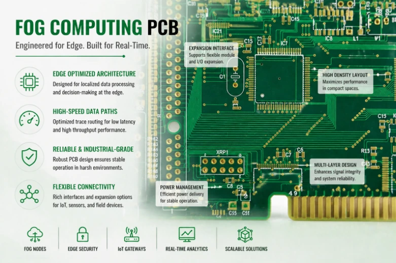
Fog nodes process and aggregate sensitive infrastructure data — industrial process parameters, utility consumption records, traffic monitoring feeds, building access logs — making them targets for both physical tampering (extracting encryption keys from a fog node mounted in an accessible cabinet) and electronic attack (intercepting or modifying data streams between sensors and cloud). PCB-level security measures form the hardware trust foundation that firmware and software protections depend upon.Hardware Security Implementation
- Secure Boot Chain: Dedicated TPM 2.0 (Infineon SLB9670) or secure element (Microchip ATECC608B) on physically isolated I²C bus with via-in-pad construction preventing bottom-side physical probing. Secure boot ROM verifying firmware signature before execution — preventing firmware replacement attacks on unattended fog nodes.
- Anti-Tamper Mesh for Critical Infrastructure: Dual-layer copper mesh (top and bottom board surfaces) connected to tamper-detection circuits in the secure element — physical intrusion (drilling, milling, or delamination attempts) breaks mesh continuity, triggering immediate erasure of encryption keys and device certificates. Required for fog nodes in critical infrastructure (utility SCADA, transportation signaling, defense networks).
- Debug Interface Security: JTAG and UART debug ports routed through zero-ohm resistor pads populated during development and depopulated during production assembly — eliminating physical debug access on deployed devices. Test pads recessed or covered to prevent casual probing.
- Side-Channel Mitigation: Power supply filtering (10 μF + 100 nF + 10 pF decoupling cascade) on cryptographic IC supply pins designed to reduce power consumption signature leakage — complicating differential power analysis (DPA) attacks on AES key schedule operations.
Environmental Durability Across Climate Zones
Fog nodes install in telecommunications cabinets in Nordic countries (-40°C winter), factory control panels in Southeast Asian tropics (40°C, 95% RH continuous), roadside traffic cabinets in desert climates (70°C inside sun-heated enclosures), and utility substations with high electromagnetic interference from power switching equipment. The PCB must survive this environmental diversity across its full 5–10 year service life — meaning the material selection, coating, and construction must address the worst-case deployment conditions, not the average.Environmental Engineering
- Thermal Stability Across Extremes: High-Tg FR-4 laminates (Tg ≥ 175°C, Td ≥ 350°C, T288 > 30 min) with low Z-axis CTE (< 3.0%/°C below Tg) — preventing delamination, via cracking, and copper foil separation under the sustained thermal stress of -40°C to +85°C daily cycling for a decade.
- Humidity and Condensation Protection: Conformal coating per IPC-CC-830 with chemistry selected for deployment climate — acrylic (AR) for indoor industrial (easy rework, adequate moisture protection), silicone (SR) for outdoor installations requiring continuous operation at 95% RH and wide temperature range, and urethane (UR) for chemical resistance in industrial environments with solvent exposure.
- Vibration Endurance for Industrial Mounting: Corner bonding adhesive on passive components ≥0805 size, capillary underfill on critical BGA packages, and SMT assembly validated through IEC 60068-2-6 random vibration testing (5–500 Hz, 2g RMS, 2 hours per axis) — meeting the vibration environment of equipment mounted on industrial machinery.
- Industrial EMI Compliance: Layout achieving IEC 61000-6-2 (industrial immunity) and IEC 61000-6-4 (industrial emissions) compliance through ground plane engineering, filtered I/O, and shielded clock distribution — without external shield cans that add cost, complicate thermal design, and require additional assembly operations.
Fleet Economics: Cost-Optimized Manufacturing at 5,000–10,000 Units
Fog computing deployments scale differently from edge or cloud — a single smart metering project deploys 5,000–15,000 identical nodes across a utility grid, a highway corridor monitoring system installs 2,000 fog gateways at 500-meter intervals, and a factory campus rolls out 500 units across 20 production lines. This fleet scale makes per-unit manufacturing cost a primary design constraint — addressed through DFM optimization and volume manufacturing efficiency rather than specification compromise.Cost-Optimized Manufacturing
- Panel Utilization Optimization: CAD-based array nesting maximizes board count per fabrication panel — optimizing board rotation, panel size selection, and routing/scoring break placement to reduce material waste by 15–30%, directly lowering per-unit cost at volumes where material is 40–50% of total board cost.
- Component Rationalization: Consolidating passive component values across design variants (standardizing on E24 preferred values, eliminating low-quantity specialty values) reduces unique BOM line items by 25–40% — improving pick-and-place throughput, reducing feeder setup time, and increasing purchasing use through larger quantities of fewer unique parts.
- Design for Automated Testing: Test pad placement for flying probe and ICT access enables 100% automated electrical testing at prototype and production stages — catching soldering defects, component value errors, and missing components before field deployment where a service visit costs $200–$500 per node.
- Turnkey Fleet Production: Integrated procurement, SMT assembly, testing, conformal coating, firmware programming, serialization, and site-specific packaging under single program management — eliminating the multi-vendor coordination overhead that inflates total cost by 15–25% and extends lead times by 3–4 weeks on fleet-scale deployments.
Fog Computing PCB FAQ
How do fog computing PCBs handle multiple wireless protocols simultaneously?
A single fog node might run Wi-Fi, BLE, LoRaWAN, and Cellular simultaneously. The PCB layout ensures coexistence without interference by using precise antenna spacing (≥λ/4), ground plane via-fencing, Dk-matched high-frequency layers, and strategic power filtering, often avoiding the need for expensive mechanical shield cans.
What PCB features protect fog node data during power outages?
Fog nodes cache critical data locally. To prevent data corruption during sudden power drops, the board incorporates supercapacitor-backed hold-up circuits, providing 100-500 ms of residual power to flush write buffers to high-endurance industrial eMMC or NVMe storage before complete shutdown.
How is hardware security implemented at the PCB level for fog nodes?
Fog nodes deployed in unattended public or industrial spaces use secure elements (like TPM 2.0), anti-tamper copper meshes that erase cryptographic keys if the board is physically breached, and zero-ohm resistor pads for debug ports that are removed before field deployment.