
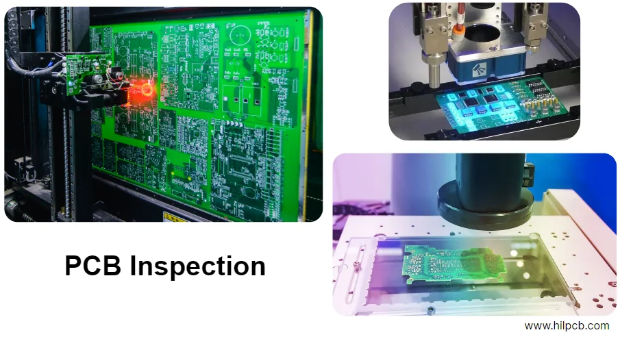
A well-designed functional test plan pcb is key to PCBA quality, reliability, and time-to-market. But from Gerber preparation to final functional validation, the full chain is full of traps. Any lapse in manufacturing, assembly, or test can cause failures, schedule slips, and cost overruns.
This guide reviews 21 common FAQs across four areas—PCB fabrication, assembly, testing, and quality management—so you can move from symptom recognition to root-cause analysis, corrective actions, and prevention. Whether you’re a design engineer, test engineer, or quality manager, you’ll find practical ways to improve yield and test efficiency.
Fabrication FAQs
Fabrication is the foundation of PCBA. Many FCT failures are rooted in bare-board defects.
1. How does PCB warpage affect functional test (FCT) accuracy?
- Symptom: The PCBA cannot sit flat in the FCT fixture; probes contact inconsistently, causing intermittent open/short miscalls.
- Metric: Per IPC-A-610, warpage after SMT assembly should be < 0.75%.
- Root causes:
- Unbalanced design: Large copper areas vs. no-copper areas are highly asymmetric.
- Stackup issues: Core and PP CTE mismatch.
- Process stress: Stress from lamination and reflow is not fully relieved.
- Fix: For produced warped boards, use baking or press-flattening equipment. This is only a rescue measure.
- Prevention:
- Design balancing: During gerber data preparation, add copper pours to balance copper distribution.
- Material choice: Select low-CTE or high-Tg laminates.
- Process control: Optimize lamination parameters and cooling to reduce residual stress.
2. Why does insufficient PTH copper thickness cause intermittent FCT failures?
- Symptom: The product fails after vibration or thermal cycling, but passes at room temperature FCT.
- Metric: IPC-6012 Class 2 requires average plated-through-hole copper thickness ≥ 20 μm.
- Root causes:
- Plating issues: Low bath activity or uneven current density.
- Drill quality: Rough hole walls or smear reduces adhesion.
- Fix: Cross-section analysis to confirm thickness. If out-of-spec, the lot is typically scrap.
- Prevention:
- Stronger monitoring: Regular bath analysis and rectifier-current monitoring.
- Better drilling: Use fresh drill bits and optimize feed/speed.
3. How do solder mask bridges that peel off or get too narrow interfere with test?
- Symptom: In dense-pin IC probing, missing bridges can short adjacent pins; mask covering pads can cause poor probe contact.
- Metric: Solder mask bridge width typically ≥ 4 mil (0.1 mm).
- Root causes:
- Insufficient exposure energy: Ink not fully cured and washes away during develop. See soldermask exposure tutorial.
- Registration errors: Film-to-board misalignment.
- Ink too thin: Excess flow narrows bridges.
- Fix: Microscopic inspection and manual touch-up for minor issues; severe cases are scrap.
- Prevention:
- Precise control: Calibrate exposure energy and alignment.
- Ink management: Control viscosity and FIFO usage.
4. What long-term risks does poor board cleanliness create for FCT?
- Symptom: FCT fails in high humidity, or leakage/shorts appear due to ECM (electrochemical migration).
- Metric: Per IPC-A-610, no visible flux residue/particles/corrosive contaminants. Ionic contamination < 1.56 μg/cm² NaCl equivalent.
- Root causes:
- Insufficient cleaning: Inadequate time/temperature or exhausted cleaner.
- Misuse of no-clean flux: Residues still risky in high-density areas.
- Fix: Ionic contamination test (ion chromatography), then ultrasonic or plasma cleaning.
- Prevention:
- Validate cleaning: Periodically verify cleaning equipment and process.
- Choose flux properly: Match flux type to environment and density.
5. How does ENIG Black Pad lead to FCT miscalls?
- Symptom: BGA/QFN PCBA shows opens in FCT, but X-Ray joints look normal.
- Metric: SEM/EDX shows excessive nickel corrosion and abnormal phosphorus content.
- Root cause: High gold-ion concentration or excessive displacement time over-attacks the nickel layer.
- Fix: Black Pad is irreversible; scrap.
- Prevention:
- Tight chemistry control: Control ENIG bath chemistry and operating parameters.
- Supplier qualification: Choose PCB suppliers with mature ENIG control.
6. How does Back-drilling depth error cause high-speed FCT failures?
- Symptom: High-speed (PCIe, USB 3.0) functional tests fail eye/BER limits.
- Metric: Stub length < 10 mil; back-drill depth tolerance within ±3 mil.
- Root causes:
- Poor depth control: Z-axis control precision issue or wrong settings.
- Thickness tolerance: Incoming board thickness deviates from assumptions.
- Fix: Not repairable; screen using TDR.
- Prevention:
- Advanced equipment: Drill machines with contact sensing or laser distance measurement.
- Design planning: Define back-drill layers and depth early.
HILPCB value: remove manufacturing barriers to test success
A successful functional test plan pcb starts with a flawless bare board. With automated pcb fabrication process steps and strict process control, HILPCB ensures copper balance, PTH plating, and surface finish quality—clearing the way for stable functional testing.
Assembly FAQs
SMT and THT assembly are high-defect zones and directly drive FCT pass rate.
7. Why do solder balls create random short failures in FCT?
- Symptom: Sporadic FCT shorts, especially after vibration or movement; hard to reproduce.
- Metric: IPC-A-610 Class 2: in 600 mm² area, ≤ 5 solder balls with diameter ≤ 0.13 mm; must not bridge non-common conductors.
- Root causes:
- Paste issues: Excess paste, slump, or moisture causing spatter.
- Bad reflow profile: Too-fast ramp in preheat boils flux and splatters solder.
- Fix: Remove visible balls with hot air and ESD brush; inspect under BGAs using X-Ray.
- Prevention:
- Paste management: FIFO, proper warm-up and mixing; optimize stencil apertures.
- Reflow optimization: Keep ramp rate ~1–3°C/s in preheat.
8. How does tombstoning cause FCT opens?
- Symptom: FCT reports opens on small chip components (0402/0201).
- Metric: One side fully lifts, forming a “tombstone.”
- Root causes:
- Uneven pad design: Different pad size or copper connection area causes thermal imbalance.
- Paste print offset: Paste doesn’t cover both pads evenly.
- Placement offset: Component is shifted to one side.
- Fix: Manual rework and re-solder.
- Prevention:
- DFM: Follow IPC-7351 pad design for thermal symmetry.
- Process accuracy: Calibrate printer and pick-and-place for accuracy.
9. What long-term risks do excessive BGA voids create, even if FCT passes?
- Symptom: FCT may pass, but failures occur in thermal cycling, vibration, or aging; thermal performance degrades and chips overheat.
- Metric: IPC-7095B suggests a single joint void area ≤ 25% of pad area.
- Root causes:
- Trapped volatiles: Flux gases trapped in molten solder.
- Moisture: PCB/components absorb moisture, vaporize during reflow, forming voids.
- Fix: Not repairable; screen strictly using x ray inspection checklist.
- Prevention:
- Reflow optimization: Extend soak time for outgassing.
- Baking: Bake MSD components and PCB before SMT.
10. How can BGA head-in-pillow (HIP) be missed by FCT?
- Symptom: Passes room-temp FCT, but fails under stress or temperature changes. X-Ray may look OK because ball and paste appear to touch.
- Metric: 3D AXI or microsection shows incomplete fusion between ball and paste.
- Root causes:
- Component/PCB warpage: At reflow peak, warpage lifts some balls away from paste.
- Paste oxidation: Low activity or too much exposure time.
- Fix: Reball or replace suspect BGA.
- Prevention:
- Warpage control: Use carriers/pallets in reflow to reduce thermal stress.
- Process tuning: Use more active paste and shorten print-to-reflow time.
11. How do selective-wave solder icicles/spikes affect FCT probe contact?
- Symptom: During THT FCT, probes can’t contact reliably; long spikes can short.
- Metric: Icicle length should be ≤ 1.5 mm and must not violate creepage/clearance.
- Root causes:
- Bad process settings: Conveyor too fast, insufficient preheat, incorrect wave height.
- Flux issues: Uneven spray or insufficient activity.
- Fix: Manually trim long spikes.
- Prevention:
- Optimize solder parameters: Tune conveyor speed, preheat, wave height, spray angle.
- Maintain equipment: Clean nozzles and ensure uniform flux application.
Is your functional test plan pcb blocked by manufacturing or assembly issues? Contact HILPCB experts—our end-to-end solutions from DFM to advanced test help you improve yield.
Test and quality FAQs
Even with perfect build quality, test design and quality control can still become failure sources.
12. What causes poor probe contact in ICT?
- Symptom: ICT reports many opens or component-value errors; retest results vary; high false calls.
- Metric: False-call rate > 5% or repeated failures at specific points.
- Root causes:
- Probe contamination/wear: Flux residue buildup or end-of-life probes.
- Poor test-point design: Too small, too close to tall parts, or covered by solder mask.
- Fixture accuracy issues: Misalignment or weak vacuum causing PCB lift/warpage.
- Fix: Clean/replace probes; inspect/clean test points; calibrate the fixture.
- Prevention:
- Better test points: Diameter ≥ 0.8 mm, pitch ≥ 1.5 mm, away from tall parts.
- Periodic maintenance: Scheduled cleaning, calibration, and replacement for probes/fixtures.
13. Why does the FCT script cause frequent false calls?
- Symptom: A known-good Golden Sample fails randomly; logs show threshold fluctuations.
- Metric: False Call Rate > 2%.
- Root causes:
- Over-tight limits: Test limits ignore component tolerance and measurement error.
- Timing issues: Script doesn’t allow enough startup/response time for the UUT.
- Environmental noise: Power noise or RFI interferes with measurement.
- Fix: Relax tolerances, add delays, and shield noise sources.
- Prevention:
- Statistical tolerance analysis: Use component specs and tester capability to set realistic limits.
- Robust scripting: Add retries and filtering.
- Test environment design: Isolated supplies and shielding enclosures for sensitive signals.
14. How do you define a reliable pass criterion for PCBA reliability tests?
- Symptom: Passes FCT but fails ESS/ALT early; unclear if design margin is insufficient or defects are random.
- Metric: A quantified criterion such as “after 1000 hours at 85°C/85%RH, key parameters degrade < 15%.”
- Root causes:
- Vague criteria: “Works normally” is not measurable.
- No application alignment: Test conditions don’t represent the harshest real use case.
- Fix: Re-evaluate product specs and application scenarios; define measurable pass/fail criteria with customers.
- Prevention:
- Build test standards early: Define reliability plans and criteria early in the project.
- Data-driven decisions: Use historical data and failure physics to set stress levels and durations.
15. Why can Hipot miscall due to humidity or residue?
- Symptom: Hipot shows breakdown/leakage over limit, but passes in a drier environment.
- Metric: Leakage readings unstable or over threshold (e.g., 5 mA).
- Root causes:
- Humidity: High humidity triggers flashover.
- Surface contamination: Flux residue, dust, fingerprints become conductive when damp.
- Fix: Bake PCBA at 60–80°C for 2–4 hours and retest under controlled humidity.
- Prevention:
- Control environment: Run Hipot at < 60% RH.
- Ensure cleanliness: Keep PCBA clean and dry before Hipot.
16. What if boundary scan coverage is insufficient?
- Symptom: Some digital faults found in FCT were missed by boundary scan.
- Metric: Coverage report shows < 90% coverage on key nets (e.g., memory data/address).
- Root causes:
- Design non-compliance: Incomplete JTAG chain or key ICs do not support boundary scan.
- Missing models: No BSDL (Boundary Scan Description Language) files for devices.
- Fix: Add vectors manually or combine with FCT to cover boundary scan blind spots.
- Prevention:
- DFT planning: Plan JTAG chain early and select boundary-scan-capable devices.
- Tool validation: Validate the schematic JTAG chain before layout.
Risk warning: an incomplete test plan is a quality gamble
A functional test plan pcb that only focuses on FCT pass/fail is far from enough. It must be a closed-loop system connecting ICT, FCT, reliability tests with manufacturing and assembly data. Ignoring early SPC warnings or traceability gaps means betting long-term reliability.
17. How should you respond when SPC charts go out of control?
- Symptom: Control charts (X-bar/R) show points beyond UCL/LCL or non-random patterns (e.g., 7 consecutive rises).
- Metric: Violation of Western Electric or Nelson Rules.
- Root cause: Special-cause variation—equipment drift, material batch change, operator error, etc.
- Fix:
- Stop production: Pause affected lines immediately.
- Quarantine product: Isolate product built after the alarm point.
- Investigate root cause: Use 5M1E analysis (man, machine, material, method, measurement, environment).
- Prevention:
- Define OCAP: Build an Out-of-Control Action Plan for each SPC alarm type.
- Train staff: Ensure operators and engineers understand SPC charts and responses.
18. How does an 8D report solve recurring FCT failures effectively?
- Symptom: The same FCT failure repeats; prior “fixes” were superficial.
- Metric: Same failure mode repeats across three consecutive lots.
- Root cause: Root Cause was never correctly identified and eliminated.
- Fix: Follow 8D rigorously:
- D1: Team formation
- D2: Problem description
- D3: Containment action
- D4: Root cause verification
- D5: Permanent corrective action selection/verification
- D6: Implement corrective action
- D7: Prevent recurrence
- D8: Recognize the team
- Prevention: Institutionalize 8D. At HILPCB, an integrated 8D data system ties failure analysis to preventive actions to stop recurrence.
19. How does incomplete traceability data impact FCT failure analysis?
- Symptom: When FCT reveals a lot issue, you can’t quickly trace the specific material batch, equipment, operator, or process parameters.
- Metric: Cannot trace full 5M1E info for a failed PCBA within 1 hour.
- Root causes:
- Insufficient data capture: Critical steps (reflow, AOI) lack barcode scanning/data capture.
- Data silos: MES/ERP/test systems are not integrated.
- Fix: Manual data collection (slow and error-prone).
- Prevention:
- Full traceability system: Unique ID and key records at every step from incoming to shipment.
- System integration: Connect production and management systems for end-to-end data flow.
20. How do you build an effective yield improvement roadmap?
- Symptom: Yield remains low; improvements are scattered and lack a system plan.
- Metric: Quarterly yield targets are missed.
- Root causes:
- Insufficient data analysis: No Pareto focus on the main defect drivers.
- No cross-functional coordination: Design/process/test/quality teams operate in silos.
- Fix:
- Collect defect data across AOI/ICT/FCT and build Pareto charts to identify top defects.
- Create cross-functional improvement teams for the top defects.
- Set SMART targets per defect (specific, measurable, achievable, relevant, time-bound).
- Review progress weekly/biweekly and adjust strategy.
- Prevention: Treat yield improvement as continuous improvement—not one-time firefighting.
21. How can poor Gerber Data Preparation create FCT risk from the start?
- Symptom: Fabricated PCB deviates from design intent and causes mass FCT failures (crosstalk, impedance mismatch, etc.).
- Metric: CAM finds > 10 DFM issues per project.
- Root causes:
- Wrong format: Non-standard Gerber output (RS-274-D instead of RS-274-X).
- Missing info: Missing drill files, stackup notes, impedance targets, or special process instructions.
- DRC violations: Minimum line/space, pad sizes exceed manufacturer capability.
- Fix: Work closely with the manufacturer’s CAM team, clarify questions, and regenerate correct Gerbers and fab data.
- Prevention:
- Use standard formats: Output RS-274-X or ODB++.
- Provide full documentation: Include a detailed Fab Drawing.
- Early DFM: Run a pre-order DFM check using manufacturer tools.
Appendix
Defect countermeasure matrix
This table summarizes common defects, related process steps, key metrics, and corrective/preventive actions.
| Defect | Process step | Key metric | Corrective / preventive action |
|---|---|---|---|
| PCB warpage | Lamination, reflow | Warpage < 0.75% | Optimize stackup, balance copper, use pallets/carriers. |
| BGA voids | SMT reflow | Void rate < 25% | Optimize profile; bake MSD parts and PCB. |
| Tombstoning | SMT placement/reflow | Zero defect | Optimize pad thermal balance; improve placement/print accuracy. |
| FCT false calls | Functional test | False call < 2% | Statistical tolerance setting; optimize test timing. |
| Black Pad | PCB (ENIG) | Zero defect | Tight bath control; strengthen supplier management. |
| Ionic contamination | Cleaning | < 1.56 μg/cm² | Validate cleaning; choose flux per product needs. |
| Icicles / bridges | Wave/selective solder | Zero defect | Optimize temperature/speed; maintain equipment. |
Quality audit checklist
Use this checklist to audit a PCBA supplier’s quality control capability.
| Audit item | Standard / requirement | Check method | Status |
|---|---|---|---|
| 1. DFM check flow | Is DFM performed on all Gerbers before production? | Review DFM reports and communication | ☐ OK ☐ NG |
| 2. Incoming inspection (IQC) | Are key components checked for spec/performance? | Review IQC records and equipment | ☐ OK ☐ NG |
| 3. MSD control | Controlled storage + baking equipment available? | On-site check and baking records | ☐ OK ☐ NG |
| 4. Paste management | FIFO, warm-up, mixing enforced? | On-site check and usage logs | ☐ OK ☐ NG |
| 5. SPI (paste inspection) | 100% SPI with SPC monitoring? | Review equipment and SPC data | ☐ OK ☐ NG |
| 6. Pick-and-place accuracy | Regular calibration in place? | Review calibration and maintenance records | ☐ OK ☐ NG |
| 7. Reflow profiling | Profiles set and validated per product? | Review profile archives | ☐ OK ☐ NG |
| 8. AOI coverage | Key joints covered and program optimized? | Review AOI programs and defect data | ☐ OK ☐ NG |
| 9. X-Ray capability | 2D/3D X-Ray for BGA FAIs and sampling? | Review equipment and reports | ☐ OK ☐ NG |
| 10. ICT platform/fixtures | Regular calibration and fixture maintenance? | Review calibration and maintenance logs | ☐ OK ☐ NG |
| 11. FCT platform control | Platform standardized and scripts version-controlled? | Review station setup and software repo | ☐ OK ☐ NG |
| 12. Test data logging | ICT/FCT data recorded and traceable? | Spot-check SNs and verify data | ☐ OK ☐ NG |
| 13. ESD control | Meets ESD S20.20? | On-site check (grounding, wrist straps, ionizers) | ☐ OK ☐ NG |
| 14. Cleanliness control | Cleaning + ionic test capability? | Review equipment and reports | ☐ OK ☐ NG |
| 15. Reliability lab | Thermal chamber, shaker, etc. available? | On-site lab check | ☐ OK ☐ NG |
| 16. SPC usage | SPC applied at key steps (SPI, reflow)? | Review SPC charts and OCAP | ☐ OK ☐ NG |
| 17. 8D system | Systematic 8D process for major issues? | Review historical 8D reports | ☐ OK ☐ NG |
| 18. Traceability system | Can trace full 5M1E? | Demo traceability query | ☐ OK ☐ NG |
| 19. Training | IPC training for operators/techs? | Review training records and certificates | ☐ OK ☐ NG |
| 20. Supplier management | Audit process for PCB/component suppliers? | Review audit reports | ☐ OK ☐ NG |
| 21. Document control | SOP/ECN controlled? | Review document-control system | ☐ OK ☐ NG |
| 22. Equipment PM | Preventive maintenance plans in place? | Review PM plan and execution | ☐ OK ☐ NG |
| 23. Packaging & shipping | ESD/moisture packaging and drop test? | Review packaging spec and test reports | ☐ OK ☐ NG |
| 24. Customer complaint handling | Clear complaint-handling flow? | Review complaint logs | ☐ OK ☐ NG |
| 25. Continuous improvement | Regular quality meetings and yield programs? | Review meeting minutes and project reports | ☐ OK ☐ NG |
HILPCB manufacturing and test capability
We’re not only a manufacturer—we’re your quality partner. HILPCB operates an advanced reliability lab, a full-traceability MES, and an experienced 8D team. We use data-driven decision-making to turn your functional test plan pcb from a document into a real execution tool, and to support a strong yield improvement roadmap.
Conclusion
A strong functional test plan pcb is much more than a list of test steps. It’s a hub that connects design, fabrication, assembly, and quality. By systematically addressing the 21 common issues above, you can reduce FCT failure rates, shorten debug time, and improve market competitiveness.
The key is prevention—not rescue. Shift quality control left: start with Gerber preparation and DFM, and enforce high standards throughout every pcb fabrication process steps. That’s how you achieve high functional-test pass rates and long-term reliability.
Ready to level up PCBA testing? Contact HILPCB for a free DFM review and test strategy consultation—let’s build a robust, high-yield product together.
For fabrication and assembly support, contact HILPCB via Turnkey Assembly or SMT Assembly for DFM/DFT guidance.
Common Questions
Why is a functional test plan more than just a checklist?
Because it connects design intent, manufacturing controls, assembly quality, and test execution into one operating system for the product. A good plan defines not only what to test, but how issues are prevented, traced, and corrected across the whole build flow.
Why should quality prevention start before FCT begins?
By the time a board reaches final functional test, many defects have already been created upstream. Starting with Gerber preparation, DFM, supplier control, and process discipline reduces the number of failures that FCT has to catch at the end.
Why do documentation, training, and equipment maintenance belong in a functional test plan?
Functional yield depends on people, procedures, and machines being consistent, not only on circuit design. Controlled documents, trained operators, and maintained equipment reduce variation and make test results more reliable and repeatable.
Why is continuous improvement important even after the test plan is established?
A plan that is never updated quickly becomes disconnected from real failure modes and production changes. Regular review of yield data, complaints, and corrective actions keeps the test strategy aligned with actual product risks.