
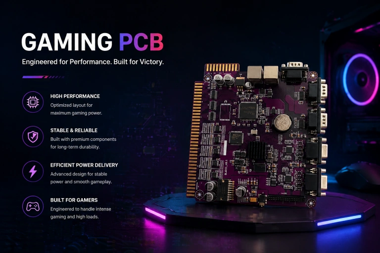
The custom mechanical keyboard community alone drives millions of PCB orders annually — enthusiasts designing open-source boards on KiCad, running group buys for 500–2,000 units, and iterating on gasket-mount flex characteristics, per-key RGB algorithms, and hot-swap socket pad geometry. Game controllers demand hall-effect joystick interfaces that eliminate stick drift, haptic feedback drivers producing textures distinguishable by touch, and wireless links achieving <4 ms latency that competitive players can feel. Console and handheld main boards route GDDR6 memory at 14+ Gbps per pin, drive HDMI 2.1 at 48 Gbps, and manage 150 W thermal loads in enclosures designed for living room aesthetics rather than airflow.
The gaming hardware market exceeds $45 billion annually, and every product category — from a $30 keyboard kit to a $500 console — depends on PCB engineering that solves problems unique to interactive electronics: latency measurable in single-digit milliseconds, physical durability under aggressive use, and visual/haptic features that differentiate products in a crowded market.
HILPCB manufactures gaming PCBs for peripheral companies, console developers, and custom hardware designers using high-speed, flex, and multilayer fabrication with impedance control, heavy copper options, and panel sizes accommodating full-size keyboard plates.
Menu Navigation
- Mechanical Keyboard PCB Engineering
- Game Controller and Input Device Boards
- Console and Handheld Main Board Design
- RGB LED Integration and Per-Key Control
- Audio and Wireless for Gaming Headsets
- Manufacturing for Gaming Products
Mechanical Keyboard PCB Engineering
Custom mechanical keyboards represent one of the highest-volume enthusiast electronics categories, with an active global design community producing both open-source and commercial PCB designs. The PCB must handle a switch matrix with N-key rollover, support hot-swap sockets for tool-free switch replacement, integrate per-key RGB, communicate over USB-C at 1 ms polling rate, and survive years of aggressive typing — including users slamming the spacebar hard enough to flex the board.
Keyboard PCB Design
- Switch Matrix Architecture: A 104-key keyboard organizes switches into a matrix — typically 6 rows × 17 columns. Each intersection has a switch and a diode (1N4148 in SOD-123 or BAV70 dual-diode for space savings). The diodes enable N-key rollover — allowing any combination of simultaneous key presses to be detected without ghosting. Matrix scanning at 1–8 kHz by the MCU (typically STM32F072, RP2040, or ATmega32U4). Trace routing for the matrix can be single-layer for simple designs or distributed across two layers on multilayer PCBs for complex layouts with per-key RGB.
- Hot-Swap Socket Compatibility: Kailh and Gateron hot-swap sockets solder to the PCB and accept MX-compatible switch pins without soldering. The socket's contact geometry requires specific pad dimensions — ±0.1 mm positional tolerance on the two switch pin pads. Through-hole pads with annular ring ≥0.25 mm to withstand 500+ switch insertion/removal cycles without pad lift. Board thickness locked at 1.6 mm (standard MX switch pin length assumes this). HILPCB's through-hole pad design maintains adhesion strength through repeated mechanical cycling.
- Board Flex and Acoustics: Keyboard enthusiasts evaluate "flex" — controlled board deflection during typing that affects keystroke feel and sound. A gasket-mount keyboard design intentionally allows 0.3–0.5 mm flex. Standard 1.6 mm FR-4 with ≥70% copper ground pour coverage provides moderate flex. Thinner boards (1.2 mm) increase flex but risk double-keystroke registration from bounce. Half-plate designs (PCB-mount stabilizers, no plate) give maximum flex — the PCB alone supports the switches and must withstand the full 60 N keystroke force without permanent deformation.
- USB-C Interface and ESD Protection: USB 2.0 full-speed at 12 Mbps for HID polling. 90 Ω differential impedance on D+/D- traces. USB-C connector footprint with reinforced through-hole mechanical tabs — the connector sees significant cable insertion/removal stress and is a leading failure point. TVS diode ESD protection (USBLC6-2SC6) within 5 mm of connector pads. CC resistors (5.1 kΩ to ground) on both CC1 and CC2 pins for proper USB-C device identification.
- MCU Selection and Firmware: QMK and VIA firmware ecosystems support STM32, RP2040, and ATmega MCUs. The PCB must expose a programming header or support USB DFU boot for firmware updates. Crystal oscillator placement within 10 mm of the MCU's XTAL pins with load capacitors (15–20 pF) within 3 mm. Ground plane continuity under the oscillator circuit prevents clock jitter that would affect USB timing.
Game Controller and Input Device Boards
Game controllers — for consoles, PC, and mobile — demand analog precision, low wireless latency, haptic feedback, and physical durability across thousands of hours of play.
Controller Board Challenges
- Hall-Effect Joystick Interface: Hall-effect joystick modules (replacing the potentiometer-based sticks that cause "stick drift") use magnetic position sensors producing analog voltage proportional to magnet displacement. The analog output (0.1–3.2 V typical) is low-bandwidth (<100 Hz mechanical bandwidth) but sensitive to noise — motor driver PWM, wireless TX bursts, and haptic driver signals can all couple into the joystick ADC input. Dedicated analog ground pour around each joystick sensor, with the ADC input traces routed on internal layers shielded from digital switching.
- Haptic Feedback Drivers: Linear resonant actuators (LRAs) driven by H-bridge ICs (TI DRV2605L, Boreas BOS1901) at 150–300 Hz with amplitude and frequency modulation creating distinct tactile textures. PWM drive signals at 20–40 kHz on internal layers to contain EMI. Separate motor supply decoupling from logic supply — haptic activation draws 100–500 mA pulses that would sag an unprotected 3.3 V logic rail.
- Low-Latency Wireless: Nordic nRF52840 or nRF5340 running proprietary 2.4 GHz protocols achieve 1–4 ms total system latency (button press to host PC registration). BLE connections add 7.5–15 ms latency. The antenna — PCB trace inverted-F or chip antenna — requires a keepout zone in the controller housing. Flex PCB extensions connect the main board to shoulder button sub-boards and trigger boards through the controller's internal cable path.
- Trigger and Button Interface: Analog triggers with 10–12 bit ADC resolution for variable input (throttle, brake in racing games). Digital buttons with <1 ms debounce — hardware RC debounce (10 kΩ + 100 nF = 1 ms time constant) or firmware debounce at the MCU's scan rate. Membrane switches on flex PCB for D-pad and face buttons.
- Battery and Charging: 1,000–2,000 mAh Li-ion pouch cell with USB-C PD charging at 5V/1.5A. CC/CV charging IC (BQ24075, MCP73831) with thermal regulation to prevent cell overheating during charging while playing. Fuel gauge IC (MAX17048) providing accurate state-of-charge estimation displayed on the controller's LED or the host system's UI.
Console and Handheld Main Board Design
Gaming consoles and handhelds integrate a custom SoC (AMD semi-custom APU for PlayStation/Xbox, NVIDIA Tegra for Switch, Qualcomm Snapdragon for mobile handhelds) with GDDR6/LPDDR5 memory, NVMe storage, display output, and wireless connectivity.
Main Board Engineering
- GDDR6 Memory Routing: 128–256 bit bus at 14–18 Gbps per pin. Trace length matching within ±0.5 mm per byte lane on low-loss laminate (Megtron 4 or equivalent). Back-drilling for via stub management on high-speed PCBs. Impedance target: 40 Ω single-ended for GDDR6 data signals.
- HDMI 2.1 / DisplayPort Output: Four differential lanes at 12 Gbps each (48 Gbps total for HDMI 2.1). 85 Ω differential impedance ±5%. Connector pad geometry per HDMI/DP licensing specs. ESD protection on all data pins without degrading signal integrity — low-capacitance TVS arrays (<0.3 pF per line).
- Multi-Phase VRM: 6–16 phase buck converter for the main SoC. DrMOS or discrete MOSFET arrays. Output capacitor bank (500–1,500 µF total distributed across 30+ ceramic and polymer capacitors) placed between VRM output and SoC power balls. IR drop across the power delivery path must be <15 mV at full load to maintain SoC voltage tolerance.
- Thermal Interface: The SoC's integrated heat spreader contacts a vapor chamber or heat pipe through thermal paste. The PCB provides mechanical mounting stiffness (12+ layer board) and supplementary heat dissipation through thermal via arrays under the SoC and VRM components. Board flatness within ±0.1 mm across the SoC contact area — maintained through balanced copper distribution and controlled lamination processes.
- Storage Interface: NVMe SSD via PCIe Gen 4 ×4. Four differential pairs at 16 GT/s — controlled impedance, back-drilled vias, and low-loss material on signal layers. M.2 connector footprint with mechanical retention and thermal pad interface to a heatsink or thermal spreader.
RGB LED Integration and Per-Key Control
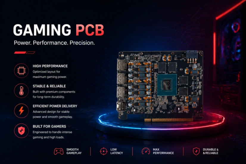
Per-key RGB on keyboards, underglow effects, and controller light bars use either addressable LEDs (WS2812B, SK6812) in series chains or LED driver ICs (IS31FL3733, IS31FL3741) controlling matrix-addressed LEDs.
LED Circuit Engineering
- Addressable LED Chains: WS2812B/SK6812 LEDs receive serial data at 800 kHz on a single data line. Each LED retransmits the remaining data to the next LED — a daisy-chain topology where one dead LED breaks the entire chain. PCB design mitigation: solder bridge pads on each LED position allowing manual bypass of a failed LED during repair. Data signal integrity is not critical at 800 kHz (λ ≈ 375 m) — signal routing constraints are mechanical, not electrical.
- Matrix-Driven LED Arrays: IS31FL3733 drives 12 × 16 = 192 LEDs over I²C — each LED individually addressable with 8-bit PWM dimming (256 brightness levels). PWM frequency: 29 kHz, eliminating visible flicker in video recordings (important for streamers). I²C bus pull-up resistors (2.2 kΩ to 3.3V) placed near the driver IC, not at the MCU — reducing I²C bus capacitance and maintaining signal rise times at 400 kHz I²C speed.
- LED Power Distribution: 104 RGB LEDs at 20 mA per color at full white = 6.24 A peak. A single 5V trace from the USB connector cannot supply this — multiple power entry points distributed across the LED array prevent voltage drop gradient that creates visible brightness variation from one end of the keyboard to the other. Typical design: four power injection points connected by 40 mil+ traces on heavy copper (2 oz) or 80 mil traces on 1 oz copper.
- EMI from LED Switching: 104 addressable LEDs switching simultaneously at 800 kHz, with additional 29 kHz PWM modulation, creates broadband emissions that can fail FCC Part 15 Class B limits. Ground plane continuity under the LED data trace, LED power supply filtering at the USB connector (ferrite bead + bulk ceramic capacitor), and proper ground return routing prevent certification failures.
Audio and Wireless for Gaming Headsets
Gaming headsets combine USB audio or wireless audio with microphone processing, sidetone mixing, and noise cancellation — on a PCB small enough to fit inside an earcup.
Headset PCB Design
- Wireless Audio Link: Proprietary 2.4 GHz dongle-based connections achieve <15 ms audio latency — critical for competitive gaming. The headset PCB carries the 2.4 GHz transceiver, codec, amplifier, and microphone preamp. Antenna placement on the headband section, away from the user's head, improves range compared to earcup mounting.
- Microphone Noise Floor: MEMS or electret microphone with 65+ dB SNR. Preamplifier and ADC supply filtered independently from the audio output path. Guard ground pour around the microphone signal conditioning circuit prevents the Class D headphone amplifier's switching noise from coupling into the microphone path.
- Active Noise Cancellation: ANC requires external microphones (on the earcup exterior), internal microphones (inside the earcup), and a DSP generating anti-noise signals in real time. The PCB routes 4–6 microphone signals with matched trace lengths (<±0.5 mm) to maintain phase coherence between channels — phase errors degrade ANC performance at higher frequencies.
- Battery Management: 500–1,500 mAh Li-ion with 30–60 hour runtime. USB-C charging with simultaneous audio operation. Charging IC selection balances charge rate with thermal constraints — the earcup's enclosed volume limits heat dissipation, so charging current must be limited to prevent the user from feeling heat on their ear.
Manufacturing for Gaming Products
Production Support
- Prototype: 10–100 boards for beta testing, community reviews, and EMC pre-compliance. Mixed SMT/through-hole for hot-swap sockets and USB-C connectors.
- Group Buy Production: 500–5,000 units for keyboard group buys and crowdfunding fulfillment. Panel optimization for keyboard PCBs (often non-standard sizes — 60%, 65%, 75%, TKL, full-size). Consistent LED color-bin matching across production lots for uniform RGB appearance.
- Volume Manufacturing: 10,000+/year for commercial gaming peripherals and console accessories. Automated functional test (USB enumeration, key matrix scan, LED verification) and reliability testing (10,000 keystroke cycles, USB connector insertion cycles).
Submit your gaming PCB design for DFM review and production quote →
Frequently Asked Questions
Why do mechanical keyboards use a switch matrix instead of individual connections? Routing each of the 100+ keys directly to the MCU would require an MCU with over 100 GPIO pins and complex routing. A switch matrix (e.g., 6 rows by 17 columns) dramatically reduces the required pin count. Diodes are added at each switch intersection to prevent ghosting and enable true N-key rollover.
How does a PCB accommodate hot-swap switches? Hot-swap PCBs use specialized sockets (like Kailh or Gateron) soldered to the board, allowing switches to be pressed in without soldering. These sockets require precise through-hole pad dimensions and reinforced annular rings (≥0.25 mm) to withstand hundreds of switch insertions without the pads lifting from the PCB.
What causes 'stick drift' in controllers, and how can the PCB fix it? Traditional analog sticks use potentiometers with physical carbon tracks that wear out over time, causing "drift." Hall-effect joystick modules solve this by using magnets and magnetic position sensors (which do not degrade from friction). The PCB must carefully route these low-voltage analog signals away from noisy digital components like wireless transceivers or haptic motors.
How do you power 100+ RGB LEDs on a single keyboard PCB? 100 RGB LEDs at full brightness can draw over 6 Amps. A single 5V trace cannot handle this without a massive voltage drop, causing LEDs at the end of the chain to appear dim or discolored. PCB designers solve this by using multiple power injection points distributed across the board, routed on heavy copper (2 oz) or extremely wide traces.