
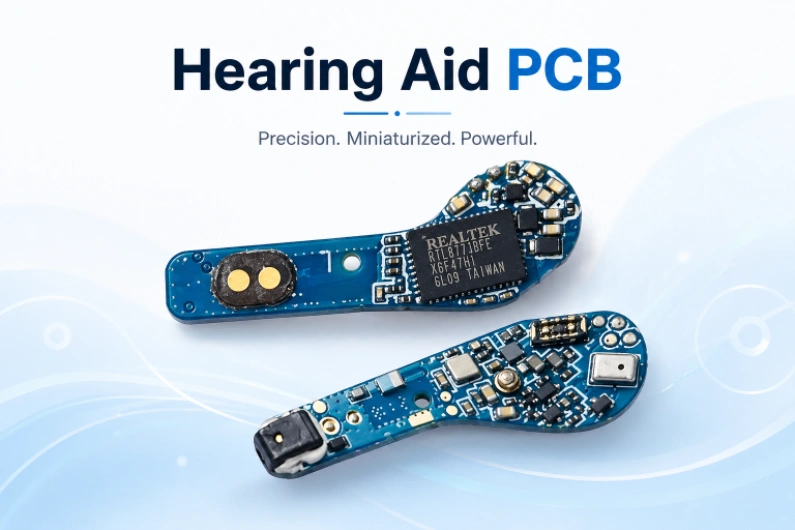
A modern receiver-in-canal hearing aid fits a dual-microphone beamforming array, a 24-bit audio DSP running real-time noise reduction and feedback cancellation, a Class D output driver, Bluetooth LE Audio streaming, rechargeable lithium-ion management, and telecoil reception — onto a PCB smaller than a fingernail. The battery budget is 1–3 mW continuous with 10–15 mW peaks during wireless streaming. Every microamp matters. Every tenth of a millimeter matters. Every milligram changes the wearing experience.
Hearing aids represent one of the most constrained electronics platforms manufactured at scale — 15+ million units shipped annually, each requiring Class II medical device compliance, biocompatible materials in contact with skin and earwax, and reliability over 5–7 years of daily wear in a warm, humid ear canal. The PCB isn't just a circuit carrier; it's a structural element that defines the device's size, weight, and ultimately patient compliance.
HILPCB produces hearing aid PCBs using HDI and flex constructions, with 01005 component capability, wire bonding for bare-die DSPs, and assembly under ISO 13485 quality systems. Our manufacturing supports layer counts up to 64 for the most complex hearing implant processor boards.
Menu Navigation
- Miniaturization at the Physical Limit
- Power Architecture for Multi-Day Battery Life
- Audio Signal Path on a Fingernail-Size Board
- Wireless Connectivity in Sub-Centimeter Packages
- Biocompatibility and Environmental Sealing
- Regulatory Manufacturing and Volume Production
Miniaturization at the Physical Limit
A completely-in-canal (CIC) hearing aid occupies roughly 1 cm³ total — PCB, battery, microphones, and receiver combined. The PCB itself is typically 6 × 8 mm or smaller, 4–6 layers, fabricated on thin-core laminates (0.3–0.5 mm total thickness).
Miniaturization Techniques
- 01005 Component Assembly: Passive components at 0.4 × 0.2 mm — requiring solder paste aperture control at ±10 µm and pick-and-place accuracy of ±25 µm. Standard stencil printing with 80 µm thick stencils and nano-coated apertures achieves consistent paste deposits at this scale. HILPCB's SMT assembly lines handle 01005 placement with machine vision verification on every component.
- Bare-Die Bonding: Hearing aid DSP chips (ON Semiconductor Ezairo, Cirrus Logic) supplied as unpackaged silicon dies — wire-bonded with 25 µm gold wire at 50–80 µm bond pad pitch, or flip-chip mounted using gold stud bumps. Eliminates package height (saving 0.3–0.5 mm) and reduces footprint by 40–60% compared to QFN packaging. Requires HDI PCB construction with fine-pitch bond pad patterns at ±15 µm positional accuracy.
- Rigid-Flex Three-Dimensional Packaging: Rigid-flex PCBs fold the electronics around the battery and receiver, accessing three-dimensional volume that a flat board cannot utilize. The flex section carries microphone connections and programming pads to an external interface. Bend radius at fold points must survive 500+ flex cycles during manufacturing and servicing without copper fatigue.
- Component-on-Both-Sides: Active and passive components placed on top and bottom board surfaces. The DSP and RF IC on one side, decoupling capacitors and matching network on the other. Shield cans (0.3 mm height clearance to tallest component) over the DSP section for EMI containment — fabricated from copper-beryllium or stainless steel, soldered to ground pads on the PCB perimeter.
Power Architecture for Multi-Day Battery Life
Zinc-air cells (1.4 V nominal, 60–312 mAh depending on size 10–675) provide 3–14 days of use. Rechargeable models use lithium-ion cells (3.7 V, 30–70 mAh) with inductive Qi charging or contact pins. Either way, every microamp of wasted current shortens the time between charges by a perceptible amount.
Ultra-Low Power Design
- Sub-µA Sleep Current: When removed from the ear (detected by capacitive proximity sensor or reed switch with battery door), the hearing aid enters deep sleep. Target: <0.5 µA total board current in sleep mode. PCB leakage through flux residue, absorbed moisture, or high-impedance traces between supply rails and ground can easily exceed this target. Post-assembly cleaning to <1.0 µg NaCl/cm² ionic contamination is mandatory. Board surface resistance between adjacent power/ground traces must exceed 10¹² Ω — verified by SIR testing on production qualification coupons.
- High-Efficiency DC-DC Conversion: Buck or buck-boost converters at 1.5–3 MHz switching frequency achieving >90% efficiency at 1 mA load — the typical active consumption. Inductor and capacitor placement within 2 mm of the switcher IC with trace widths maintaining <50 mΩ loop resistance. Switching noise filtered through ferrite beads (impedance >100 Ω at 100 MHz) before reaching the audio ADC and DAC supply rails. The ferrite bead + ceramic capacitor filter corner frequency must sit above the switching frequency but well below the audio ADC's sampling clock.
- Inductive Charging Interface: Rechargeable hearing aids use a charging coil (∅8–12 mm, typically 10–20 turns) integrated on a flex extension or separate module within the charging case. The PCB traces forming the secondary receiving coil must maintain ±0.1 mm dimensional accuracy for consistent coupling efficiency with the case's primary coil. Qi-compatible designs operate at 110–205 kHz with rectification and regulation on the hearing aid PCB.
- Battery Protection: Over-charge (4.2 V cutoff), over-discharge (2.7 V cutoff), and over-current (200 mA limit) protection ICs with <0.5 µA quiescent current — protecting both the cell and the patient (lithium cell failure in an ear canal is a safety concern). Cell voltage monitoring through high-impedance dividers (10 MΩ + 10 MΩ) that contribute <0.2 µA to the quiescent drain.
Audio Signal Path on a Fingernail-Size Board
Two MEMS microphones → analog front end → 24-bit sigma-delta ADC → DSP (adaptive noise reduction, binaural beamforming, acoustic feedback cancellation, audiogram-based frequency shaping, compression) → DAC → Class D micro-driver → balanced armature receiver. This entire chain runs at 16–24 kHz sample rate with <5 ms group delay — the threshold above which users perceive their own voice as delayed and unnatural.
Audio PCB Discipline
- Microphone Signal Integrity: MEMS microphones output either analog (requiring low-noise preamp on the PCB) or PDM digital (requiring a clean clock and data path to the DSP). In either case, the microphone traces are the most noise-sensitive paths on the board. Guard ground pours surround microphone routing to prevent capacitive pickup from the BLE radio's TX bursts, the switching regulator, or the DSP's clock harmonics. Physical separation ≥3 mm between microphone traces and any digital bus.
- DSP Power Domain Isolation: The hearing aid DSP contains both digital core (operating at 1–20 MHz clock) and analog codec (ADC + DAC). These require separate, independently filtered supply rails. Even on a 6 mm board, dedicated LDO regulators for digital core (0.9–1.2 V) and analog codec (1.8 V) with individual 100 nF + 1 µF decoupling prevent digital switching noise from modulating the DAC output — which manifests as a faint buzzing or hissing heard by the patient.
- Receiver Driver Considerations: Balanced armature receivers present complex impedance (30–100 Ω, highly reactive at audio frequencies). The Class D output filter must be tuned for this load — not the resistive 4–8 Ω speaker load that IC reference designs assume. An LC filter designed for 8 Ω will overshoot and ring into a 32 Ω reactive load, creating audible distortion and potentially damaging the receiver.
- Feedback Path Management: Acoustic feedback (the whistle heard when a hearing aid's microphone picks up its own amplified output) is managed in the DSP, but the PCB can make it worse. Mechanical coupling between the receiver and microphone through the PCB substrate transmits vibration at acoustic frequencies. Mounting the microphone on a flex extension, mechanically decoupled from the main board, reduces this substrate-borne feedback path.
Wireless Connectivity in Sub-Centimeter Packages
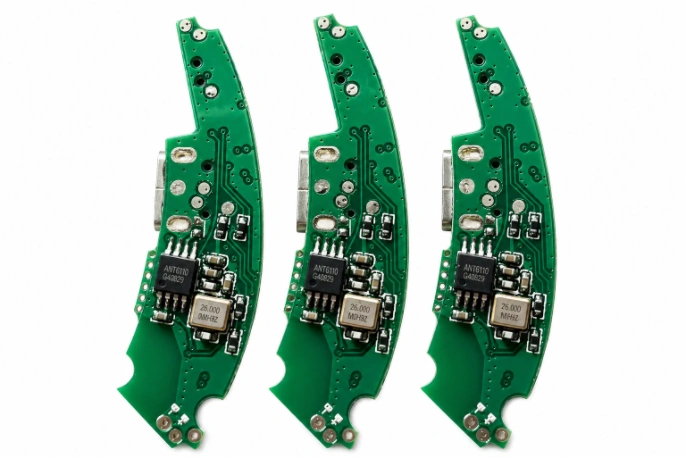
Bluetooth LE Audio (LC3 codec at 32 kHz sample rate) enables direct streaming from smartphones, TV streamers, and Auracast public broadcast systems. The antenna must operate at 2.4 GHz within a device worn inside or behind the ear — surrounded by lossy biological tissue that absorbs RF energy and detunes the antenna.
Wireless Design Challenges
- Antenna in Body Proximity: The human head absorbs and detunes 2.4 GHz antennas significantly — typical free-space designs lose 6–15 dB of gain when placed against the ear. Antenna design must include a head phantom model (SAM head per IEEE 1528) during simulation. Ground plane size — often only 5 × 8 mm — limits achievable gain to -5 to -15 dBi. Every dB of antenna gain saved is a dB of transmit power (and therefore battery drain) not needed.
- Compact Antenna Integration: Chip antennas (2.0 × 1.25 mm, e.g., Johanson 2450AT18D0100) or PCB trace antennas (inverted-F or meander line) occupying the board edge. The antenna element requires a keepout zone — no copper pour, no components, no traces within approximately 3 mm in all directions. On a 6 × 8 mm board, this antenna keepout zone consumes 30–40% of the board area — it's the single largest constraint on component placement.
- Radio-Audio Coexistence: BLE radio generates broadband noise during TX bursts (0 dBm typical output, 1–2 ms burst duration). This noise couples into the audio ADC input through supply rails, ground plane currents, and near-field radiation. Mitigation: supply filtering between radio and audio domains, physical separation, and TX scheduling that avoids transmitting during the ADC's sampling aperture — requiring coordination between the DSP firmware and the BLE stack.
- Telecoil Reception: Hearing loop systems in theaters, churches, and public spaces transmit audio via magnetic induction at 3.15 kHz ±10% carrier frequency. The telecoil — either a wound copper coil on a ferrite core or a PCB trace spiral on a dedicated layer — receives this signal. The telecoil must be oriented perpendicular to the ground (vertical when the user is standing) and shielded from the switching regulator's magnetic field, which operates at a frequency (1–3 MHz) that's close enough to create interference through harmonic mixing.
Biocompatibility and Environmental Sealing
Hearing aids operate in the ear canal — an environment with cerumen (earwax), perspiration, body temperature, and occasional exposure to rain, shower spray, and cosmetic products. The PCB must survive this for 5–7 years without corrosion, delamination, or performance degradation.
Environmental Protection
- Nano-Coating: Hydrophobic plasma-deposited fluoropolymer coatings (0.1–1 µm thick) applied to the assembled PCBA after testing. These invisible coatings repel moisture and cerumen without blocking acoustic ports or affecting electrical contacts. The coating process must not contaminate battery contacts, charging contacts, or programming pads — masking or selective deposition is required.
- Material Compliance: All PCB materials meet IEC 60601-1 requirements. High-Tg laminates with moisture absorption <0.1% (per IPC-TM-650) prevent dimensional changes from humidity cycling in the ear canal environment. Lead-free SAC305 solder with halogen-free laminate and solder mask — confirmed by ISO 10993-5 cytotoxicity testing for skin-contact medical devices.
- IP68 Water Resistance: Premium hearing aids claim IP68 water resistance (submersion to 1 m for 30 minutes). The PCB itself doesn't provide this protection — the device housing does — but the board must survive the moisture that inevitably penetrates seals over years of use. Conformal coating (acrylic or parylene) on the assembled PCBA provides secondary moisture protection.
- Corrosion-Resistant Surface Finish: ENIG (electroless nickel immersion gold) on all exposed copper provides corrosion resistance in the humid ear canal environment. Immersion tin or OSP finishes tarnish within months under these conditions and are not suitable.
Regulatory Manufacturing and Volume Production
Medical Device Manufacturing
- Class II Medical Device: Hearing aids are FDA Class II (De Novo or 510(k) pathway), EU Class IIa under MDR. PCB fabrication and assembly under ISO 13485 quality systems with full lot traceability and change control. HILPCB maintains ISO 13485 certification supporting hearing aid OEM qualification requirements.
- Prototype Development: 10–50 units for DVT/EVT with design history file documentation. Quick-turn prototypes using production-equivalent materials and processes to ensure prototype-to-production consistency.
- Volume Production: IPC-6012 Class 3 fabrication for medical reliability. Component authentication from authorized distributors with lot-date traceability. SMT assembly with automated optical inspection and functional testing including acoustic output measurement and wireless link verification.
- Yield Optimization: At 01005 component density on a 6 × 8 mm board, first-pass yield depends critically on solder paste printing quality. SPI (solder paste inspection) on 100% of boards before placement, with real-time feedback to the printer for aperture-level volume correction. Target: >98% first-pass SMT yield at these component densities.
Launch your hearing aid PCB program with our medical miniaturization team →
Frequently Asked Questions
How small can components get on a hearing aid PCB? Hearing aid PCBs utilize 01005 passive components, which measure just 0.4 × 0.2 mm. Placing these requires extreme precision: ±10 µm solder paste aperture control and ±25 µm pick-and-place accuracy. Additionally, the main DSPs are often mounted as bare-die silicon directly bonded to the board to save vertical space.
Why is moisture protection so critical for hearing aid PCBs? Hearing aids operate inside the ear canal—a warm, humid environment containing sweat and cerumen (earwax). To prevent corrosion and electrical leakage over a 5-to-7-year lifespan, the assembled PCB is coated with hydrophobic plasma-deposited fluoropolymers or parylene conformal coatings that repel moisture without blocking acoustic components.
How does the PCB design affect hearing aid battery life? Hearing aids must run for days on tiny batteries. If the PCB has even 1 microamp of leakage current—caused by flux residue or poor trace isolation—it perceptibly shortens battery life. The board is designed for a sub-microamp sleep state, using ultra-high-efficiency DC-DC converters and requiring extreme post-assembly cleaning to eliminate ionic contamination.
What challenges does Bluetooth integration bring to hearing aid PCBs? Adding Bluetooth LE to a 6x8 mm board introduces two massive problems: antenna tuning and RF noise. The antenna requires a large "keepout zone" free of copper, consuming up to 40% of the board space. Furthermore, the human head absorbs RF energy, detuning the antenna. The PCB must also strictly isolate the BLE radio's transmission bursts to prevent them from inducing audible buzzes in the sensitive microphone circuits.