
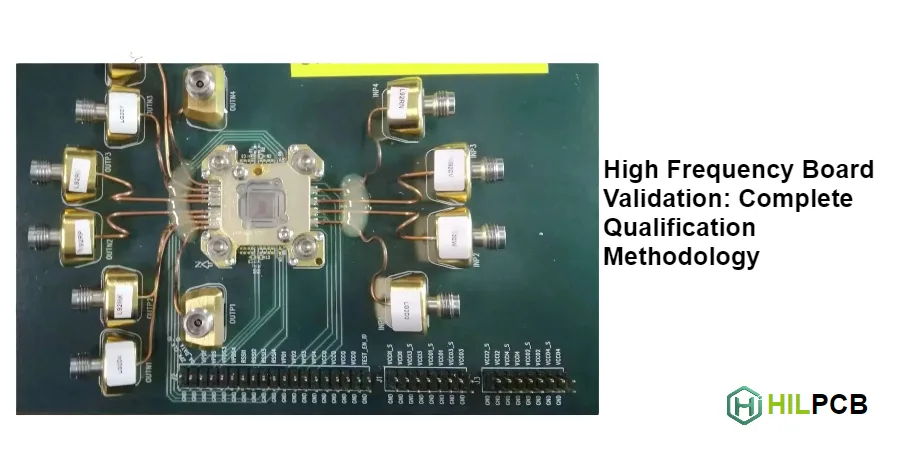
High-frequency board validation is the evidence-based process used to show that a fabricated PCB meets its defined electrical, material, structural, and documentation requirements before production release. It connects design intent to measurable bare-board results without treating a coupon test as proof of assembled-product or system compliance.
Key Takeaways
- Separate design validation, bare-board qualification, PCBA verification, and final system release; each has different owners and evidence.
- Write acceptance limits, reference planes, bandwidth, test vehicles, and measurement uncertainty before choosing equipment or sample quantities.
- Correlate material data, field-solver predictions, fabricated coupons, bare-board measurements, assembled channels, and system results rather than substituting one for another.
- A TDR result verifies impedance versus time or distance; a VNA result characterizes frequency-domain transmission and reflection. Neither automatically proves end-product compliance.
- Define lot sampling and requalification triggers from risk, procurement documents, applicable standards, and process history—not a universal percentage or Cpk target.
Table of Contents
- What does high-frequency board validation prove?
- Define acceptance before selecting tests
- Build a correlation ladder
- High-frequency board validation release matrix
- How should impedance and loss be validated?
- What material and construction evidence is needed?
- How should sampling and requalification be controlled?
- Common validation failures
- High-frequency PCB validation RFQ checklist
- What can HILPCB support?
- Frequently asked questions
What Does High-Frequency Board Validation Prove?
Validation is useful only when its scope is explicit. A bare-board test can show that a manufactured transmission-line structure matches an agreed requirement, but it cannot certify receiver margin, antenna performance, EMC, environmental durability, or regulatory compliance for the finished product.
| Scope | Primary question | Typical evidence | Normal owner |
|---|---|---|---|
| Design validation | Does the modeled interconnect meet its budget? | Solver/channel model and sensitivity analysis | Customer design/SI team |
| Bare-board qualification | Did fabrication reproduce the specified construction and electrical behavior? | Stackup, representative coupons, specified electrical data, microsections | Fabricator; customer approves |
| PCBA/product verification | Did assembly and components preserve performance? | Assembled-channel or functional tests | Customer, assembler, or laboratory |
| System release | Does the final product meet application and compliance requirements? | System/compliance reports and release authorization | Product manufacturer or qualified laboratory |
Avoid requesting “complete validation” without defining the measurand, boundary, and release authority.
Define Acceptance Before Selecting Tests
An acceptance statement must be reproducible by another competent party. “Pass impedance” is incomplete; it needs a target, tolerance, structure, measurement window, reference condition, and disposition rule. The same principle applies to insertion loss, return loss, mode conversion, isolation, dimensions, plating, and structural integrity.
For each requirement, record:
- Limit source: drawing, interface specification, model budget, or procurement standard.
- Quantity, units, port notation, reference plane, frequency/time window, and board condition.
- Coupon or on-board structure and its relationship to the production feature.
- Calibration, fixture characterization, de-embedding, gating, and reporting settings.
- Sample selection, disposition, retest rules, and approval authority.
There is no universal ±5% or ±10% impedance tolerance, return-loss threshold, crosstalk limit, environmental profile, sample percentage, or process-capability index that releases every high-frequency PCB. These values become requirements only when the applicable design and procurement documents make them requirements.
Build a Correlation Ladder
The strongest release case is a chain of correlated evidence, not a single certificate or instrument trace.
| Evidence level | What it contributes | Why it is not interchangeable with the next level |
|---|---|---|
| Material supplier data | Method-, axis-, frequency-, and condition-specific properties | May not represent the real circuit field or frequency |
| Solver/channel model | Predicted impedance, loss, delay, and sensitivity | Reflects inputs, not the finished construction |
| Fabricated coupon | Controlled structure built with the panel process | Represents selected geometries, not the routed board |
| Bare-board measurement | Pre-assembly electrical or construction evidence | Excludes connectors, components, and assembly variation |
| Assembled-channel measurement | Launches, vias, traces, connectors, and components together | May not exercise the complete product environment |
| System performance | Final application or compliance result | Can expose failure without isolating its cause |
Rogers guidance shows why correlation matters: Dk and Df depend on method, axis, frequency, and construction, while copper roughness affects loss and propagation. A material certificate is an input—not proof of circuit Dk or channel performance.
High-Frequency Board Validation Release Matrix
Use this matrix as a project-specific control sheet. Replace every “agreed” entry with an actual drawing note, numeric limit, or referenced procedure before release.
| Requirement | Measurand / vehicle | Reference and measurement method | Acceptance rule | Lot strategy and evidence | Requalification trigger | Owner |
|---|---|---|---|---|---|---|
| Controlled impedance | Single-ended/differential coupon | TDR reference, bandwidth, probe, window, board condition | Target/tolerance by class | Coupon trace linked to panel/lot | Stackup, material, copper, compensation, or process change | Fabricator; customer approves |
| Insertion/return loss | Two-/four-port coupon or channel | VNA plane, fixture removal, ports, sweep, gating | Frequency-dependent channel/RF budget | Touchstone plus setup record | Launch, connector, material, copper, via, or geometry change | Customer/SI team or laboratory |
| Differential balance | Differential structure/channel | Mixed-mode S-parameters and port orientation | Project mode-conversion/skew rule | Raw data and settings | Pair geometry, registration, or assembly change | Customer/SI team |
| Construction | Coupon/board microsection | Approved location and method | Drawing/procurement standard | Images and measured geometry | Drill, plating, lamination, via-fill, or supplier change | Fabricator |
| Material identity | Laminate, bondply, foil, finish | Purchase, lot, and supplier records | Approved material/equivalent | CoC and lot records | Grade, factory, resin, foil, or thickness change | Fabricator/customer |
| Continuity/isolation | Production netlist | Agreed electrical-test rules | Procurement documentation | Lot status and disposition | Netlist, program, or process change | Fabricator |
| PCBA channel | Assembled vehicle/product | Defined fixture/system method | Interface/product requirement | Report tied to build revision | Component, connector, process, or layout change | Customer/assembler |
| Environment/compliance | Finished product/qualified assembly | Application plan at qualified facility | Named product/regulatory requirement | Controlled report/approval | Design, process, supplier, or environment change | Product manufacturer/laboratory |
How Should Impedance and Loss Be Validated?
TDR and VNA measurements answer complementary questions. TDR is effective for controlled-impedance verification and locating discontinuities in time or distance. VNA S-parameters show transmission, reflection, and—on suitable multiport setups—differential/common-mode conversion versus frequency.
A representative coupon should reproduce the production layer, dielectric, copper, geometry, reference planes, solder-mask condition, and processing. It needs a panel/lot identity. Branched or inaccessible on-board traces can add launch, return-path, and termination effects that obscure fabrication behavior.
For VNA work, calibration establishes a defined reference plane; de-embedding removes characterized lead-ins and lead-outs beyond it. The report should identify calibration, ports, probes/cables, fixture method, sweep, relevant IF bandwidth, gating, renormalization, and transformation. Measurement uncertainty belongs to the analyzer–setup–DUT system, not the analyzer alone.
Retain raw and processed Touchstone files when S-parameters support release; screenshots without setup metadata are not reproducible evidence.
What Material and Construction Evidence Is Needed?
High-frequency performance is sensitive to interacting variables: dielectric thickness, etched conductor shape, copper profile, resin/glass distribution, material anisotropy, plated geometry, solder mask, via stubs, and reference-plane continuity. Validation should therefore pair electrical results with construction evidence rather than trying to infer every cause from a single trace.
Useful evidence can include approved material and foil identification, supplier lot documents, as-built stackup, microsection measurements, drill/plating records, impedance-coupon results, and agreed insertion-loss data. For Rogers PCB or PTFE PCB constructions, the RFQ should also state whether substitutions are prohibited and which supplier property value or customer model governs design correlation.
How Should Sampling and Requalification Be Controlled?
Sampling is a risk decision. Base it on the procurement specification, product criticality, destructive versus nondestructive method, lot definition, panel representation, measurement capability, prior process performance, and customer approval. Do not copy a generic “2–5%,” “100% impedance,” or Cpk threshold from another program.
Define requalification before the first lot. Typical triggers include changes to material grade or source, copper foil profile, dielectric thickness, stackup, controlled geometry, artwork compensation, lamination cycle, drill or plating process, via structure, surface finish, coupon design, test fixture, calibration method, manufacturing site, or an adverse trend/nonconformance. The change review decides which earlier evidence remains valid and which tests must be repeated.
Common Validation Failures
| Failure | Why the evidence is weak | Better release control |
|---|---|---|
| Datasheet Dk lacks method/frequency | Model may use the wrong property | Record source, method, axis, frequency, and correlation |
| Coupon passes; routed board fails | Coupon omitted a launch, via, transition, or asymmetry | Correlate a design vehicle or assembled channel |
| VNA trace lacks reference plane | Fixture/cable effects cannot be separated | Document calibration and fixture removal; retain raw data |
| TDR average hides a discontinuity | One number masks launch/via behavior | Retain waveform and declared window |
| Environmental profile is copied | Stress may be irrelevant or insufficient | Derive it from product requirements |
| Supplier change uses the same material label | Construction or process Dk may differ | Perform equivalence review and requalification |
High-Frequency PCB Validation RFQ Checklist
Design and files
- Gerber/ODB++ or IPC-2581 data, drill files, netlist, drawing, stackup, controlled-impedance table, and revision identifiers.
- Transmission-line geometry, reference layers, copper/finish requirements, via/backdrill details, and prohibited substitutions.
Electrical requirements
- Impedance classes and tolerances; S-parameter notation and limits versus frequency; required ports, fixtures, calibration plane, de-embedding, and file format.
- Coupon structures, panel locations, board-versus-coupon testing, data retention, and correlation vehicle.
Material, quality, and release
- Exact laminate/bonding/foil designations, governing Dk/Df source, material traceability, microsection requirements, applicable performance class, sampling plan, report format, and approval owner.
- Lot definition, nonconformance/retest rules, record retention, change notification, and requalification triggers.
What Can HILPCB Support?
For high-frequency PCB manufacturing, HILPCB can review fabrication inputs, align the proposed stackup and coupon with procurement notes, and define the agreed inspection and lot-document package. Confirm exact TDR, insertion-loss, VNA, environmental, or laboratory deliverables in the quotation.
HILPCB's fabrication role does not replace customer design authority, assembled-channel verification, regulatory assessment, or product release. For external testing, specify method, accreditation scope, data ownership, and acceptance authority.
Reference Standards and Guidance
- IPC-6018 — IPC
- IPC-6012 — IPC
- IPC-2221 — IPC
- IPC-TM-650 — IPC
- IEEE 370 — IEEE
- ISO/IEC 17025 — ISO/IEC
Frequently Asked Questions
Does a passing impedance coupon prove the board will pass system testing?
No. It verifies represented transmission lines. System performance also depends on routing, vias, connectors, components, assembly, receiver behavior, firmware, and environment.
Is TDR or VNA better for high-frequency board validation?
Neither is universally better. TDR profiles impedance and locates discontinuities; a VNA measures frequency-domain S-parameters. Select by measurand and correlate when needed.
Should every controlled-impedance PCB receive 100% impedance testing?
Not automatically. “100%” could mean every coupon, panel, lot, board, or impedance class. State the sampling unit and acceptance plan.
Can a material certificate validate Dk and Df for my circuit?
It confirms documented material information, but usable Dk/Df depends on method, axis, frequency, copper, and construction. Correlate it with a solver and fabricated vehicle.
When should a high-frequency PCB be requalified?
Use predefined triggers: material, stackup, copper, geometry, process, supplier, site, coupon, or measurement-method changes, plus adverse trends. Agree which evidence must repeat.
Release With Evidence, Not Assumptions
High-frequency board validation succeeds when each requirement has a representative measurement, traceable setup, acceptance owner, and requalification rule. Send HILPCB the stackup, validation matrix, coupon requirements, and data-package expectations for a manufacturing review and quotation.