
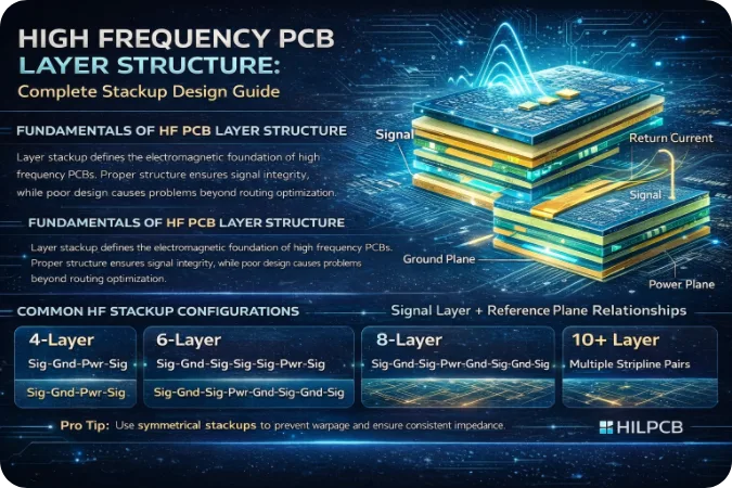
A high-frequency PCB stackup is the controlled arrangement of copper and dielectric layers that defines each transmission line, its return path, coupling, loss and manufacturability. It must be frozen with the fabricator before routing because the final pressed dielectric, copper profile and fabrication tolerances—not a generic layer template—set the electrical result.
Key Takeaways
- “High frequency” is not one clock threshold. For digital nets, edge rate and interconnect delay determine transmission-line behavior; for RF, use the carrier, harmonics and modulation bandwidth.
- Give every critical signal a continuous adjacent reference and a local return path at each layer transition. A differential pair still interacts with its reference planes.
- Choose microstrip, stripline or grounded coplanar waveguide from loss, isolation, launch, routing and fabrication needs rather than assuming one is always superior.
- Use the laminate supplier's design data at the relevant frequency and structure. Nominal data-sheet Dk alone is not enough for an impedance or phase model.
- Include pressed thickness, copper thickness/profile, etch compensation, solder mask, glass weave and via geometry in the field solver.
- Specify separate acceptance evidence for impedance, insertion loss, dimensions and material identity. TDR impedance testing does not prove an RF channel's complete loss or launch performance.
Table of Contents
- What makes a PCB stackup high frequency?
- Which requirements must be frozen before layer count?
- How should signal and reference planes be paired?
- Microstrip vs stripline vs grounded coplanar waveguide
- How should 4-layer, 6-layer and 8-layer stackups be used?
- How should laminate, Dk and loss be specified?
- How do vias, launches and plane changes affect the stackup?
- What manufacturing and test evidence is required?
- Common high-frequency stackup failure modes
- High-frequency PCB stackup RFQ checklist
- Frequently asked questions
What Makes a PCB Stackup High Frequency?
The stackup becomes electrically critical when a trace can no longer be treated as an ideal connection. Fast digital edges propagate as waves even when the clock frequency looks modest. RF and microwave circuits are directly sensitive to impedance, phase length, loss, coupling and discontinuities at their operating frequencies.
Do not classify every net by a broad “above 100 MHz” rule. Record instead:
- digital driver rise/fall time, interface standard, voltage and allowed timing or eye degradation;
- RF frequency range, bandwidth, power, noise figure or matching sensitivity;
- impedance mode and target, including single-ended, differential or coplanar geometry;
- maximum routed length, allowable insertion/return loss and phase or skew budget;
- connector, package, via and test-launch models that belong to the channel.
Layer count then follows routing density, plane continuity, BGA escape, power distribution, isolation, mechanical thickness and fabrication capability. A two-layer RF board can be valid for a focused microstrip circuit. A dense mixed-signal product may need many layers. “RF boards must be at least four layers” is not an engineering requirement.
Which Requirements Must Be Frozen Before Layer Count?
The following requirement-to-evidence matrix prevents a stackup from becoming a drawing that no one can verify.
| Design requirement | Stackup consequence | Manufacturing variable | Release evidence |
|---|---|---|---|
| characteristic impedance | trace width/space, copper thickness and distance to reference | pressed dielectric, etch and plating | field-solver model plus TDR coupon results |
| insertion-loss budget | material Df, copper profile, geometry and length | laminate lot, oxide/bond treatment and conductor roughness | VNA coupon/channel data with defined fixture removal |
| phase or delay matching | effective Dk, line length and weave exposure | resin content, glass style and registration | matched-line or delay measurement where required |
| crosstalk limit | layer assignment, spacing and reference coupling | finished trace width/space and layer registration | simulation plus representative measurement if risk justifies it |
| RF launch/transition | pad, antipad, via barrel, stub and return-via placement | drill, plating, backdrill depth and registration | launch model, microsection and VNA structure |
| board flatness/reflow | symmetric material and copper distribution | lamination cycle and copper balance | stackup construction record and bow/twist acceptance |
| target thickness | core/prepreg selection and foil build | prepreg flow and copper density | finished-board and dielectric measurements |
Start the discussion with the fabricator's stocked core, prepreg, copper foil and qualified lamination combinations. A mathematically attractive construction that requires unavailable glass styles or an unqualified hybrid bond is not a production stackup.
How Should Signal and Reference Planes Be Paired?
High-frequency return current concentrates in the nearby reference structure because that path minimizes loop inductance. A route over a plane split, void or board edge forces the field to spread and find a longer path, increasing discontinuity, coupling and radiation.
Use these rules during stackup and placement:
- Put each critical routing layer next to a continuous reference plane.
- Keep the same reference under the complete route where practical.
- When a signal changes layers but keeps the same reference net, place a return via close to the signal via.
- When the reference changes between ground and power, provide a low-inductance return path between those references at the transition, usually with appropriately placed capacitance according to the PDN design.
- Do not route critical signals across split planes. Separating functional areas by placement and controlled current paths is safer than cutting the reference beneath them.
Differential coupling does not make reference continuity optional. Tightly coupled pairs share more field with each other, but some field still terminates on surrounding planes and copper. Include the actual reference geometry, pair spacing and asymmetry in the solver.
Plane-pair capacitance is useful only when the power and ground planes are close enough and have suitable area and dielectric properties. A common four-layer construction may have a thick L2-to-L3 core, so simply labeling those layers “ground” and “power” does not guarantee meaningful high-frequency plane capacitance.
Microstrip vs Stripline vs Grounded Coplanar Waveguide
No transmission-line structure wins every trade-off.
| Structure | Advantages | Costs and risks | Good fit |
|---|---|---|---|
| microstrip | direct component launch, easy probing/tuning, part of field travels in air | more exposure to adjacent structures, solder-mask sensitivity and radiation at discontinuities | short RF routes, antennas, filters and top-side components |
| stripline | field contained between planes, strong isolation and predictable reference environment | more dielectric loss, via transitions, difficult tuning and possible broadside coupling | long internal digital/RF routes and isolation-sensitive channels |
| grounded coplanar waveguide | lateral grounds can control field and support via fencing/launches | impedance depends on gap, ground continuity and via-fence geometry; poor implementation creates resonances | RF launches, compact matching networks and surface RF routing |
Stripline does not have “no radiation”; discontinuities, slots, vias and connectors can still radiate. Orthogonal routing on adjacent signal layers can reduce one coupling mechanism but does not replace adequate spacing and plane shielding. For broadside overlap, the safest control is usually a larger separation, a reference plane between layers or deliberate routing exclusion.
The solver must use finished geometry. Outer-layer traces are plated and etched differently from inner layers, solder mask changes microstrip behavior, and trapezoidal trace shape matters when features are small.
How Should 4-Layer, 6-Layer and 8-Layer Stackups Be Used?
These examples are starting architectures, not released dimensions.
Four layers
| Layer | Example role |
|---|---|
| L1 | components and critical microstrip |
| L2 | solid ground reference |
| L3 | power regions and low-speed routing, kept continuous under any L4 critical routes |
| L4 | low-speed signals or selected routes referenced to L3 |
This structure works well when most critical routing stays on L1 over L2. If L4 also carries fast signals, L3 must be designed as a reliable reference rather than a fragmented power layer.
Six layers
| Layer | Example role |
|---|---|
| L1 | signal/components |
| L2 | ground |
| L3 | signal referenced primarily to L2 |
| L4 | signal referenced primarily to L5 |
| L5 | ground |
| L6 | signal/components |
Use a comparatively larger L3-to-L4 separation to reduce broadside coupling. Power can be routed as controlled regions or wider conductors on appropriate layers, supported by the PDN analysis. Calling L3 and L4 “stripline” without identifying their actual reference planes and spacing is incomplete.
Eight layers
| Layer | Example role |
|---|---|
| L1 / L8 | component-side microstrip and low-density routing |
| L2 / L7 | ground references |
| L3 / L6 | critical internal signals |
| L4 | ground or additional reference |
| L5 | power distribution |
An eight-layer design provides more choices for isolated internal routing and a closer power/reference pair. The final ordering may change with BGA escape, power-domain count and RF placement. Keep construction and copper distribution sufficiently balanced around the centerline to control bow and twist.
How Should Laminate, Dk and Loss Be Specified?
Material selection starts with a channel budget, not a generic frequency table. Ordinary FR-4 families vary widely; “Dk 4.3, Df 0.020” is not a universal FR-4 model. Likewise, no single GHz threshold makes PTFE mandatory.
Ask for these material inputs:
- exact laminate and prepreg family, glass style, resin content and nominal/pressed thickness;
- design Dk appropriate to the transmission-line structure, frequency and supplier method;
- Df or measured loss data over the relevant range;
- copper foil type/profile and the fabricator's bonding treatment;
- z-axis CTE, Tg/Td, moisture and thermal-cycle suitability;
- qualified substitutes and the electrical revalidation required before a change.
Rogers distinguishes Design Dk values intended for circuit modeling from values produced by other material test methods. Its differential-phase-length approach uses two microstrip lines and can show Dk versus frequency. The broader lesson applies to every supplier: record which Dk, method, frequency and structure entered the model.
At multi-gigabit and microwave frequencies, conductor roughness can add loss and alter phase behavior. Glass-weave geometry can create local Dk variation and differential skew when the two traces sample different glass/resin regions. Mitigations include spread-glass materials, routing angle, wider pair geometry or stricter material control, chosen from the actual skew budget.
Hybrid high-frequency PCB stackups can place low-loss material only around sensitive RF layers, but the cost advantage is not an automatic 40–60%. The fabricator must qualify bonding, resin fill, material movement, drilling, desmear, copper treatment, registration and thermal expansion across the mixed system.
How Do Vias, Launches and Plane Changes Affect the Stackup?
A via is not a zero-length connection. Its barrel inductance, pad capacitance, antipad, unused stub and nearby return vias form a discontinuity whose severity depends on frequency and transition geometry.
For every critical transition, define:
- start/end layers and unused barrel length;
- finished hole, pad, antipad and capture-pad geometry;
- return-via count and position;
- connector or package launch dimensions;
- whether backdrilling, blind vias or another stub-control method is required;
- breakout, registration and fabrication limits that preserve the modeled geometry.
Backdrilling should follow a modeled or measured stub budget, not a blanket rule. Confirm drill-to-copper clearance, remaining stub, registration and inspection method. For a dense multilayer PCB, the best layer order may be the one that shortens critical via transitions even if another arrangement looks cleaner on paper.
What Manufacturing and Test Evidence Is Required?
Release the stackup as a controlled data set rather than a colored diagram.
| Characteristic | Recommended evidence | What it does not prove |
|---|---|---|
| impedance | field-solver record and TDR coupon with limits | end-to-end insertion loss or connector launch quality |
| insertion/return loss | VNA coupon or channel measurement with defined calibration/de-embedding | every routed product trace unless correlation is established |
| dielectric thickness | microsection or qualified process data | laminate identity by itself |
| copper/etch geometry | finished trace/coupon dimensions and microsection where required | electrical performance without material data |
| material identity | certificate/lot traceability and controlled substitute list | pressed thickness after lamination |
| via/backdrill | microsection, X-ray or depth-control record as applicable | RF performance without a correlated test structure |
TDR is the established production method for controlled-impedance coupons. The coupon must reproduce the relevant layer, dielectric, copper and geometry, and its location/panel representation must be agreed. At frequencies where insertion loss matters, use an appropriate test coupon and VNA method; IEEE 370 provides interconnect characterization and de-embedding guidance.
Allow the fabricator to propose trace-width compensation using its finished-process model, but require approval of any change that affects spacing, coupling or layout clearance. “50 ohms ±5%” is not a substitute for defining structure, coupon, test method, lot sampling and disposition rules.
Common High-Frequency Stackup Failure Modes
| Symptom | Likely stackup cause | Discrimination check |
|---|---|---|
| impedance coupon passes but channel loss fails | rough copper, high Df, long route or poor launch | VNA coupon/channel separation and material/foil review |
| prototype works, production shifts phase | Dk method, resin content, glass style or material substitution | lot traceability plus matched-line phase measurement |
| emissions spike after a layer change | broken return path, longer via stub or altered plane resonance | return-current audit and near-field/TDR localization |
| differential eye closes despite correct impedance | skew, loss imbalance, via asymmetry or crosstalk | mixed-mode S-parameters and pair geometry review |
| board bows after reflow | asymmetric build, copper imbalance or hybrid material movement | construction/copper-density review and bow/twist data |
| RF match changes after solder mask update | altered microstrip/CPWG effective geometry | re-solve with actual mask thickness/Dk and measure |
High-Frequency PCB Stackup RFQ Checklist
Electrical requirements
- interface or RF band, rise time, channel length and power level;
- single-ended/differential impedance, tolerance and target structures;
- insertion loss, return loss, phase/skew and crosstalk budgets at stated frequencies;
- connector, package, via, launch and reference-transition requirements.
Construction and material
- layer functions, finished thickness, copper weights and symmetry constraints;
- exact laminate/prepreg or approved electrical/thermal equivalence criteria;
- design Dk/Df source, copper profile, solder-mask model and glass-weave control;
- via, antipad, backdrill, sequential-lamination and registration limits.
Verification and change control
- TDR coupon structures, limits, sampling and report format;
- insertion-loss coupon/method, fixtures, calibration and de-embedding;
- microsection, material certificate and lot/press-panel traceability;
- fabricator compensation authority, substitute approval and requalification triggers;
- quantities, panel constraints, assembly thermal profile and retained samples.
HILPCB can review a controlled stackup, impedance structures, via transitions, coupons and fabrication notes before quoting prototype or production fabrication. Add small-batch assembly or turnkey PCB assembly requirements only when the RF launch, cleaning, solder, inspection and test responsibilities are also defined.
Reference Standards and Specifications
- IPC-2221 — IPC
- IPC-2222 — IPC
- IPC-2141 — IPC
- IPC-6012 — IPC
- IPC-6018 — IPC
- IPC-TM-650 2.5.5.7 — IPC
- IEEE 370 — Institute of Electrical and Electronics Engineers
Use the revisions, performance class and test methods agreed for the released product.
Frequently Asked Questions
Is a four-layer PCB enough for high-frequency design?
It can be. A four-layer board with critical top-layer routing over a solid L2 ground is effective for many focused designs. The decision depends on routing density, transitions, power distribution, isolation and loss—not frequency alone.
Is stripline always better than microstrip?
No. Stripline offers field containment but adds dielectric loss and vias. Microstrip simplifies launches, tuning and probing and can have lower dielectric loss. Choose from the complete channel and manufacturing constraints.
Should every differential pair be routed without a plane split?
Yes, keep its reference environment continuous. Pair coupling does not eliminate plane interaction, and a split can create common-mode conversion, return-path discontinuity and emissions.
Can nominal data-sheet Dk be used directly in the impedance solver?
Only when the supplier confirms that value and method are appropriate to the structure and frequency. Record design Dk, frequency, test method, resin/glass construction and the fabricator's pressed thickness.
Does a passing TDR coupon prove the RF board is good?
It proves the coupon's impedance met the stated method and limits. It does not by itself prove insertion loss, launch return loss, differential mode conversion or every product trace.
What should be approved before routing begins?
Approve the fabricator-supported layer construction, materials, pressed thicknesses, copper profiles, modeled impedance geometries, via rules, reference transitions and coupon/test plan.
Freeze the Stackup as an Electrical and Manufacturing Contract
A publishable layer diagram is not enough. A robust high-frequency stackup links every channel requirement to a modeled geometry, a qualified material/process variable and a measurable acceptance record. Freeze that contract with the fabricator, then route against the released values and control every later substitution through electrical revalidation.