
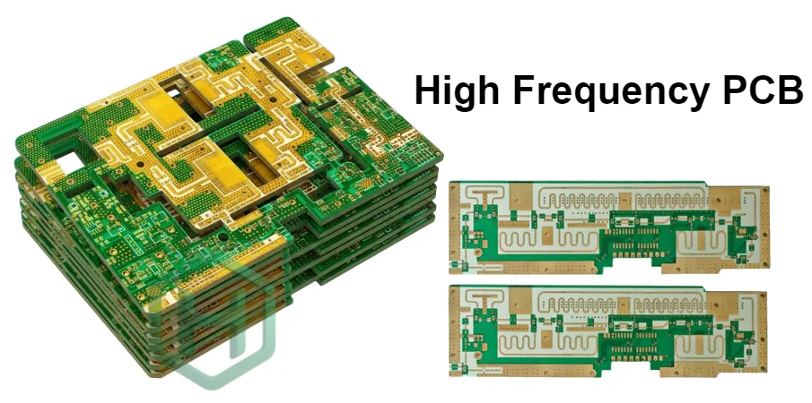
High-frequency PCBs sit at the intersection of RF performance, reliability engineering and operations management. A design that looks good in simulation still has to survive fabrication tolerances, assembly stress, field conditions and long-term supply-chain changes. This guide looks at high-frequency PCBs from a lifecycle perspective: how to invest wisely, adopt new technologies, control risk, protect reliability and build a supply chain that scales with your product.
To make it easier to navigate, this article is organised into five technical sections:
- Managing High-Frequency PCB Investment Across the Product Lifecycle
- High-Frequency PCB New Technologies and Customisation Strategies
- Addressing High-Frequency PCB Challenges from Design to Production
- Reliability, Lifetime, Maintenance and Upgrades in High-Frequency PCBs
- High-Frequency PCB Mass Production, Services and Supply Chain Competitiveness
1. Managing High-Frequency PCB Investment Across the Product Lifecycle
For serious RF and high-speed systems, high-frequency PCB investment is not just a question of unit price per panel. It is a strategic decision that affects performance margin, field reliability, upgrade flexibility and overall lifecycle cost. The right investment strategy aligns material and process choices with business goals: performance targets, production volume, time-to-market and long-term support.
At HILPCB, we structure high-frequency PCB investment around the complete product lifecycle—from early prototypes to stable mass production—so engineering decisions made today do not become financial or technical bottlenecks tomorrow.
Key Investment Focus Areas
- Performance vs. Cost Balancing Prioritizing low-loss materials, controlled impedance and robust stackups where they actually improve RF performance, while using cost-effective options in non-critical regions. For complex architectures this often means combining RF-optimised layers with cost-effective logic and power layers inside a single multilayer PCB build.
- Lifecycle-Oriented Stackup Decisions Selecting materials and structures that are available and stable for years, so redesigns are not forced by obsolescence or sourcing shifts in the high-frequency PCB supply chain. In many cases this is based on material sets already proven in our high-frequency PCB production lines.
- Prototyping vs. Volume Tuning Using premium options for first articles when needed, but converging toward configurations that a high-frequency PCB mass-production manufacturer can run reliably and economically.
- Risk Mitigation as Investment Treating design-for-manufacturability reviews, test coupons and early process characterization as part of high-frequency PCB investment, because they significantly reduce re-spin and field-failure costs.
- Customisation with Clear Payback Applying high-frequency PCB customization—special stackups, launches, embedded structures, or locally using advanced dielectrics such as Teflon PCB—only where the performance gain, integration benefit or lifetime improvement is measurable.
Consistent Return on High-Frequency PCB Investment
By linking technical decisions to quantifiable outcomes—performance margin, yield, field-return rate and upgrade flexibility—HILPCB helps OEMs treat high-frequency PCB investment as a managed asset rather than a sunk cost. The result is a board platform that supports the product roadmap, not just the first release, and can be manufactured, serviced and scaled without repeated reinvention.
2. High-Frequency PCB New Technologies and Customisation Strategies
High-frequency PCB new technologies are expanding rapidly, driven by 5G/6G, satellite links, automotive radar and high-speed computing. At the same time, every project has its own constraints and signal profiles. The challenge is to apply new techniques and materials in a way that is technically sound, manufacturable, and justifiable from a business perspective.
HILPCB combines process capability with application knowledge to turn innovation into practical high-frequency PCB customisation, rather than one-off experiments.
Key Technology and Customisation Topics
- Advanced Low-Loss and Hybrid Materials Integrating low-loss laminates, PTFE-based cores and hybrid RF + FR-4 stacks where they directly benefit attenuation, phase stability and bandwidth.
- HDI and Fine-Feature Structures Using blind/buried vias, via-in-pad and tight line/space only where density or signal integrity requires it, while keeping the overall process robust for batch production.
- Embedded RF Structures Implementing embedded couplers, filters and impedance transformers in copper and dielectric as part of the high-frequency PCB overall solution, reducing external components and interconnect loss.
- Band- and Application-Specific Tuning Tailoring stackups, launches and shielding concepts to particular bands (sub-6 GHz, mmWave, radar bands) instead of forcing one generic approach across all products.
- Design Rules for Custom Platforms Defining clear, repeatable rule sets so high-frequency PCB customization can be applied across a product family—rather than re-solving the same integration problems each time.
Consistent Innovation with Manufacturable Outcomes
By aligning new technology adoption with clear design rules and proven processes, HILPCB enables OEMs to integrate high-frequency PCB new technologies without sacrificing manufacturability or schedule. Customisation becomes a structured capability—backed by a high-frequency PCB service provider that can support both engineering builds and long-term product families.
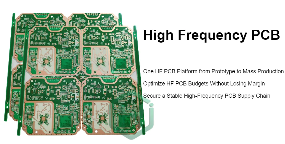
3. Addressing High-Frequency PCB Challenges from Design to Production
Every serious RF or high-speed project faces a set of recurring high-frequency PCB challenges: reconciling simulation with fabrication limits, controlling variability, and keeping performance stable as the design moves from lab prototypes to production lines. These challenges span design, process and test; no single team can solve them alone.
HILPCB tackles high-frequency PCB challenges as an integrated engineering problem, bringing layout, process engineering and test experience into one feedback loop.
Key Challenge Areas
- Model vs. Reality Alignment Ensuring that stackup, Dk/Df and copper assumptions used in simulation are consistent with real materials, process tolerances and high-frequency PCB technical requirements.
- Geometry and Process Tolerances Managing line width, spacing, dielectric thickness and via registration so impedance and loss stay inside the specified window across many production lots.
- Thermal and Mechanical Stress Controlling lamination cycles, reflow profiles and mechanical constraints so high-frequency PCB reliability and lifetime are preserved, even under harsh operating conditions.
- Assembly-Induced Performance Drift Accounting for shields, connectors, housings and rework when designing launches and RF-sensitive areas, reducing detuning and parasitic effects introduced during assembly and maintenance.
- Cross-Team Communication Gaps Bridging the gap between RF engineers, layout designers, process engineers and test teams, so high-frequency PCB common issues are anticipated and prevented instead of discovered late.
Consistent Mitigation of High-Frequency PCB Challenges
Through structured DFM reviews, controlled process windows and targeted test strategies, HILPCB turns high-frequency PCB challenges into known, manageable factors rather than surprises. This approach shortens debug cycles, stabilizes production behaviour and supports high-frequency PCB troubleshooting and repair when complex systems are already in the field.
4. Reliability, Lifetime, Maintenance and Upgrades in High-Frequency PCBs
In telecom, automotive, aerospace and industrial systems, high-frequency PCB reliability is as critical as initial performance. Failures can be costly, dangerous or both. Reliability engineering must therefore consider not only the first power-on, but the long-term high-frequency PCB lifetime, maintenance, repair and upgrade path.
HILPCB designs and manufactures high-frequency boards with the full operational lifecycle in mind, not just the acceptance test.
Key Reliability and Lifecycle Topics
- Material and Stackup Stability Selecting dielectrics, copper systems and finishes that maintain RF characteristics over temperature, humidity and time, and that support the desired high-frequency PCB lifetime.
- Via and Interconnect Robustness Engineering via structures, aspect ratios and plating to withstand thermal cycling, vibration and assembly stresses, reducing latent failure risks.
- Serviceability and Maintenance Design Providing access for high-frequency PCB maintenance and repair—test points, modular architecture, connector strategies—so field technicians can work efficiently.
- Structured Troubleshooting and Repair Paths Supporting high-frequency PCB troubleshooting with reference S-parameter data, known-good signatures and rework guidelines for sensitive RF components and launches.
- Planned Upgrade Capability Designing for high-frequency PCB upgrades: spare connectors, reserved routing channels, and stackup margin that allow new bands, higher data rates or additional channels without full redesign.
Consistent Field Performance and Long-Term Support
By embedding reliability, maintainability and upgrade strategies into the high-frequency PCB overall solution, HILPCB helps customers reduce field failures, simplify service operations and extend product lifetimes. This approach turns the PCB into a stable platform for future evolution instead of a disposable, single-generation asset.
5. High-Frequency PCB Mass Production, Services and Supply Chain Competitiveness
As products transition from engineering pilots to sustained shipments, attention shifts from individual boards to the robustness of the high-frequency PCB supply chain. At this stage, the strength of your high-frequency PCB mass-production manufacturer and service ecosystem becomes a direct competitive factor.
HILPCB positions itself as a high-frequency PCB service provider and supply-chain partner, not just a board vendor—coordinating technology, volume, logistics and lifecycle support.
Key Supply Chain and Service Elements
- Scale-Up from NPI to Volume Using the same qualified processes from prototypes through pilot runs into mass production, maintaining consistent behaviour while capacity increases. Early-stage runs can be supported on flexible small-batch assembly lines before volume migrates to higher-capacity cells.
- Coordinated Full-Scope Solutions Providing high-frequency PCB full-scope solutions that integrate fabrication, assembly, test and logistics into a single high-frequency PCB holistic solution, simplifying management and responsibility. For system-level delivery, this includes box-build assembly and full turnkey assembly, so PCB, PCBA and enclosure integration are handled by one team.
- Supplier Redundancy and Risk Control Structuring material sources, capacity planning and contingency options so single points of failure are minimized within the high-frequency PCB supply chain.
- Transparent Service and Communication Offering clear channels for high-frequency PCB consulting, status updates, deviation handling and continuous improvement, rather than treating production as a black box.
- Competitiveness in Cost and Capability Combining cost control with technical depth, so the high-frequency PCB mass-production manufacturer remains competitive on price while still meeting demanding RF and reliability requirements.
Consistent, Competitive High-Frequency PCB Delivery
By treating high-frequency PCB production as a supply-chain and service problem—not just a factory output—HILPCB helps OEMs achieve predictable lead times, stable quality and responsive support. This integrated approach to high-frequency PCB investment, technology, reliability and supply chain is what ultimately drives sustainable high-frequency PCB competitiveness in demanding markets.
Common Questions
Why should a high-frequency PCB program be managed across the full product lifecycle instead of only around the first prototype?
Because the real risk is rarely just whether the first sample works. The harder challenge is whether the design can be reproduced, maintained, and supplied consistently over time, and those lifecycle issues often surface only after the prototype stage.
What is the most common mistake when introducing new high-frequency technology?
Teams often stack new materials, new structures, or new frequency requirements into one program without defining clear design rules and manufacturable limits at the same time. The technology itself may be sound, but without a controlled validation path it quickly becomes difficult to scale.
Why should maintenance and future upgrades be considered early in reliability planning?
Many high-frequency products stay in service for years and later need connector changes, band extensions, or localized repair. If the original design leaves no room for test access, interface strategy, or stack-up margin, every later maintenance action becomes more expensive and risky.
Why does supply-chain strength directly affect competitiveness in the production phase?
Because by the time a product reaches recurring production, customers are buying dependable delivery, not just a technically good board. If material sourcing, capacity flexibility, service response, or long-term support are unstable, even a strong prototype result will not translate into sustained business success.