
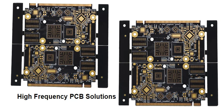
What separates professional high frequency PCB manufacturing from basic RF capability is material expertise selecting optimal substrates for frequency and performance requirements, fabrication process controls maintaining tight impedance tolerances, thermal management for high-power RF circuits, and validation testing confirming electrical performance across frequency ranges. The challenge extends beyond using Rogers materials—it requires complete engineering solutions optimizing signal integrity, minimizing losses, and ensuring manufacturability.
HILPCB reviews custom RF PCB builds that specify low-loss materials such as Rogers 4350B, RO3003, RO4003C, and other high-frequency laminates. The review covers stack-up, impedance, fabrication, assembly, and the validation plan for applications including 5G, automotive radar, satellite communications, and defense electronics. Exact material, capability, and delivery timing are confirmed for the quoted construction.
Minimizing Insertion Loss in High Frequency PCB Designs
Signal loss in RF and microwave circuits directly impacts system performance—reducing receiver sensitivity, limiting transmitter range, and degrading signal-to-noise ratios. At multi-gigahertz frequencies, even short trace lengths exhibit measurable insertion loss from dielectric absorption and conductor losses that conventional PCB materials cannot adequately control.
At HILPCB, our low loss high frequency pcb material selection and design optimization minimize insertion loss enabling maximum RF performance for high frequency pcb for telecom infrastructure, rf pcb for 5g applications, and radar systems where every decibel of loss affects system capabilities.
Key Loss Minimization Techniques
Low-Loss Laminate Selection: Rogers RO4350B (Df=0.0037 @ 10GHz), RO3003 (Df=0.0013 @ 10GHz), and other low loss high frequency pcb materials provide dramatically lower dielectric losses than FR4 (Df>0.02), essential for microwave pcb solutions operating above 5GHz.
Copper Surface Roughness Optimization: Smoother copper foils (RTF or HVLP rather than standard electrodeposited) reduce skin-effect losses at high frequencies, critical for high speed rf pcb applications where conductor losses dominate above 10GHz.
Dielectric Thickness Control: Thinner dielectrics for controlled impedance reduce field penetration into lossy materials while minimizing trace length for given impedance, optimizing high frequency pcb fabrication performance.
Via Transition Optimization: Minimizing via length, optimizing barrel diameter, and eliminating via stubs reduces parasitic inductance and capacitance degrading signals at transitions in custom rf pcb solutions.
Trace Width and Spacing Optimization: Balanced geometry achieving target impedance while minimizing conductor loss through adequate trace width for rf pcb fabrication service designs operating across wide frequency ranges.
Ground Plane Continuity: Solid, uninterrupted ground planes minimize return path losses and maintain controlled impedance, essential for microwave pcb fabrication requiring predictable electrical characteristics.
Insertion Loss Validation
S-parameter measurement using vector network analyzers (VNA) characterizes insertion loss (S21) across operating frequency ranges, validating designs meet system budgets. HILPCB provides measured S-parameter data on test coupons or production boards supporting customer system integration for high frequency pcb for telecom and aerospace applications. This validation capability differentiates professional high frequency pcb manufacturer services from basic Rogers material lamination.
Achieving Tight Impedance Control for RF Circuit Performance
Impedance accuracy and consistency determine RF circuit performance—affecting matching network effectiveness, filter characteristics, and power transfer efficiency. At high frequencies, impedance variations from material tolerances, fabrication variations, and environmental changes degrade circuit performance requiring rigorous controls during design and manufacturing.
For a build using a specified Rogers laminate, HILPCB reviews impedance geometry and process controls against the released stack-up. The quoted tolerance, coupon design, test method, and production evidence must be agreed before fabrication.
Key Impedance Control Techniques
Material Dielectric Constant Stability: Rogers laminates maintain consistent Dk across frequency (RO4350B: Dk=3.48±0.05) and temperature, enabling predictable impedance compared to FR4 where Dk varies significantly with frequency and moisture for custom rf pcb solutions.
Precise Dielectric Thickness Control: Manufacturing process controls maintaining dielectric thickness within ±0.7 mils (±18μm) ensure impedance accuracy, critical for microwave pcb solutions where small thickness variations create significant impedance deviations.
Copper Thickness Uniformity: Electroplating process controls delivering uniform copper thickness across panels prevent impedance variations from copper weight deviations in rf pcb fabrication service production.
Etch Factor Optimization: Controlled etching processes achieving consistent trace sidewall profiles ensure impedance uniformity across trace widths and lengths for high frequency pcb fabrication quality.
TDR Impedance Verification: Time-domain reflectometry measurement on production test coupons validates impedance meets specifications (typically ±5-10%), providing documented verification for high speed rf pcb applications.
Temperature Coefficient Management: Material selection considering temperature coefficient of dielectric constant (TCDk) minimizes impedance variation across operating temperature ranges for rf pcb for 5g applications deployed in outdoor environments.
Impedance Design Tools and Validation
Electromagnetic simulation using 2.5D/3D field solvers (Ansys HFSS, Keysight ADS) enables accurate impedance prediction accounting for material properties, geometric effects, and frequency-dependent phenomena. HILPCB provides impedance modeling support and measured impedance data validating fabrication meets design intent for high frequency pcb prototype validation and production verification.

Managing Thermal Performance in High-Power RF Circuits
RF power amplifiers, transmitters, and high-power radar systems generate significant heat requiring effective thermal management preventing performance degradation and reliability failures. High frequency PCB materials typically exhibit lower thermal conductivity than standard FR4, while compact RF designs concentrate heat in small areas challenging thermal dissipation.
At HILPCB, thermal engineering integrated into microwave pcb solutions and rf pcb for 5g applications ensures stable performance and long-term reliability for high-power RF circuits across telecommunications and aerospace applications.
Key Thermal Management Techniques
Thermally Enhanced Laminates: Rogers RO4350B (thermal conductivity 0.69 W/m·K) and TMM laminates (0.80-1.44 W/m·K) provide better thermal performance than standard PTFE materials, critical for high frequency pcb for telecom power amplifiers.
Metal-Core Integration: Aluminum or copper core substrates integrated with low loss high frequency pcb surface layers provide superior heat extraction for high-power applications, common in custom rf pcb solutions for base station power amplifiers.
Thermal Via Arrays: Dense via patterns beneath high-power RF devices transfer heat from active surface through dielectric to metal core or heat sink, essential for GaN and GaAs power amplifiers in rf pcb fabrication service assemblies.
Copper Plane Heat Spreading: Maximum copper coverage on internal layers within routing constraints spreads localized heat across larger circuit area, reducing peak temperatures in microwave pcb fabrication designs.
Component Placement Thermal Optimization: Strategic placement of heat-generating components (power amplifiers, mixer diodes, voltage regulators) prevents thermal clustering while positioning devices near thermal extraction paths for high frequency pcb manufacturer designs.
Heat Sink Integration Design: PCB layout facilitating attachment of heat sinks, cold plates, or forced-air cooling ensures effective thermal management in complete rf pcb assembly service implementations.
Thermal Validation and Reliability
Infrared thermal imaging during RF operation identifies hotspots requiring design optimization, while thermal cycling testing validates reliability under operational temperature swings. HILPCB's thermal engineering ensures high speed rf pcb assemblies maintain electrical performance across temperature ranges while surviving accelerated life testing, supporting long-term reliability for high frequency pcb for telecom infrastructure requiring 15-20 year operational lifetimes.
Optimizing Layer Stackups for Mixed-Signal RF Designs
Modern RF systems integrate digital control, analog signal processing, and high-power RF sections on single boards requiring careful stackup design preventing digital noise coupling into sensitive RF circuits while maintaining controlled impedance for RF signal paths.
At HILPCB, mixed-signal expertise integrated into custom rf pcb solutions enables clean RF performance coexisting with digital processing for rf pcb for 5g applications, software-defined radio, and instrumentation requiring both RF and digital functionality.
Key Mixed-Signal Stackup Techniques
RF Section Isolation: Dedicated ground planes separating RF sections from digital circuits prevent coupling through shared reference planes, essential for microwave pcb solutions maintaining clean RF performance alongside FPGA or processor control circuits.
Selective Material Usage: Combining low loss high frequency pcb materials (Rogers, TMM) in RF sections with cost-effective FR4 in digital areas optimizes performance while controlling costs for cost effective rf pcb manufacturing.
Power Supply Partitioning: Separate power planes or segmented planes for RF and digital supplies prevent switching noise coupling from digital sections into sensitive RF low-noise amplifiers in high frequency pcb fabrication designs.
Shielding Integration: Grounded shield traces or guard rings surrounding RF sections provide additional isolation from digital noise sources, critical for receiver front-ends in high frequency pcb for telecom applications.
Digital Section Grounding: Star grounding or plane segmentation in digital sections prevents digital return currents coupling into RF ground references for rf pcb fabrication service quality.
Layer Count Optimization: Adequate layers enabling dedicated RF signal routing, isolated ground planes, and separate power distribution without routing compromises supports high speed rf pcb signal integrity across both RF and digital domains.
Mixed-Signal Validation
Spectrum analyzer measurements during digital operation verify RF section noise floor remains acceptable, while EMI testing confirms digital section emissions don't interfere with RF receive bands. HILPCB's mixed-signal expertise enables custom rf pcb solutions achieving RF performance specifications while integrating complex digital control and signal processing required for modern telecommunications systems.

Enabling Cost-Effective High Frequency PCB Manufacturing
High frequency PCB materials historically commanded significant cost premiums over FR4 due to specialty laminate pricing and fabrication complexity. However, competitive dynamics, material availability improvements, and manufacturing optimization enable cost effective rf pcb solutions expanding high-frequency technology adoption beyond premium applications.
At HILPCB, manufacturing efficiency and design collaboration deliver high frequency PCB economics supporting rf pcb for 5g applications in cost-sensitive markets while maintaining performance and reliability requirements.
Key Cost Optimization Strategies
Selective High-Frequency Material Usage: Using Rogers or other premium materials only where RF performance demands while employing standard FR4 for digital sections, power supplies, and control circuits reduces overall material costs in custom rf pcb solutions.
Material Grade Selection: Choosing appropriate material grade balancing performance and cost (RO4350B for general RF vs. RO3003 for ultra-low-loss applications) optimizes value for application requirements in high frequency pcb fabrication.
Standard Thickness Utilization: Leveraging fabricator-stocked material thicknesses rather than custom orders reduces lead time and material costs for rogers pcb manufacturer processing.
Design for Manufacturability: Early engagement identifying fabrication-friendly approaches (standard trace widths, conventional vias rather than blind/buried where adequate) improves yield and reduces cost for rf pcb fabrication service production.
Volume-Scaled Pricing: Material cost amortization and setup cost spreading across production volumes significantly improves economics, with transparent pricing across quantity breaks supporting customer planning.
Panel Utilization Optimization: Efficient board layout maximizing panels reduces material waste and per-unit costs, particularly significant for smaller RF modules in microwave pcb fabrication applications.
Economic Viability for Broader Applications
Through these optimization strategies, HILPCB enables high frequency PCB adoption in applications previously using discrete RF components on FR4 or expensive ceramic substrates. Cost effective rf pcb manufacturing expands Rogers material benefits into automotive radar (77GHz collision avoidance), consumer 5G devices, IoT wireless systems, and industrial sensors where RF performance advantages justify moderate cost premiums over FR4. Our high frequency pcb supplier position delivers these economics while maintaining quality standards required for automotive and telecommunications applications.
Accelerating Development with High Frequency PCB Prototype Service
RF circuit design involves iterative optimization of matching networks, filter responses, and amplifier performance making prototyping essential for validating electrical performance before production commitments. Traditional high-frequency prototype lead times of 2-3 weeks create development bottlenecks in competitive wireless markets.
At HILPCB, high frequency pcb prototype services deliver functional RF boards in 7-10 days with validated electrical performance, enabling rapid design iteration for custom rf pcb solutions development across telecommunications and aerospace applications.
Key Rapid RF Prototyping Capabilities
Quick-Turn Rogers Fabrication: Streamlined processing and material inventory enable fast turnaround for standard Rogers laminates (RO4350B, RO4003C) supporting high frequency pcb prototype responsiveness.
Design Rule Verification: Expert RF-specific DFM review within 24 hours identifies high-frequency design issues (impedance calculations, via transitions, ground plane continuity) before fabrication for rogers pcb manufacturer quality.
Flexible Minimum Quantities: Low MOQ (5-10 pieces) makes RF prototyping economically viable for early-stage development, with transparent pricing supporting budget planning for microwave pcb solutions projects.
Material Variety Access: Availability of multiple Rogers products, TMM laminates, and other specialty materials enables material selection validation during prototyping for rf pcb fabrication service applications.
Electrical Testing Capability: S-parameter measurement services on prototypes provide performance validation before volume production commitments for high speed rf pcb development.
Assembly Integration: Combined rf pcb assembly service with prototype fabrication delivers tested RF modules in 10-14 days total, accelerating functional validation for rf pcb for 5g applications development.
Development Velocity Advantages
Rapid RF prototyping particularly benefits products where wireless performance differentiates competitive positioning and regulatory compliance testing requires validated designs. HILPCB's high frequency pcb manufacturer responsiveness enables agile RF development with multiple design iterations within compressed schedules, critical for 5G infrastructure, automotive radar, and consumer wireless devices where product generations cycle rapidly and time-to-market determines market share capture.
Professional RF PCB Assembly Service for High-Frequency Circuits
RF circuit assembly presents unique challenges beyond standard SMT: component placement accuracy affects matching network performance, soldering technique impacts RF ground connections, and handling prevents ESD damage to sensitive RF devices. Professional assembly expertise ensures fabrication quality translates to functional RF performance.
At HILPCB, rf pcb assembly service capabilities address RF-specific requirements through precision equipment, optimized processes, and validation testing ensuring assembly quality for high frequency pcb for telecom and aerospace applications.
Advanced RF Assembly Capabilities
High-Precision Component Placement: Tight placement accuracy (±25μm) ensures RF component orientation and positioning meets design intent for matching networks and filter implementations using SMT assembly technology.
RF Connector Assembly Expertise: Precision soldering of coaxial connectors (SMA, 2.92mm, 2.4mm) ensuring proper ground connection and center conductor alignment critical for microwave pcb solutions operating above 10GHz.
ESD-Protected Handling: Controlled ESD environment protecting sensitive RF components (GaAs amplifiers, mixer diodes, voltage-controlled oscillators) from assembly-induced damage in custom rf pcb solutions processing.
Specialized Reflow Profiling: Thermal profiles optimized for Rogers and TMM laminates preventing substrate degradation while ensuring complete solder reflow for low loss high frequency pcb assemblies.
Shield Can Attachment: Precision placement and soldering of RF shield cans providing electromagnetic isolation between circuit sections for high speed rf pcb performance.
Testing and Tuning Services: RF functional testing, matching network tuning, and power calibration services deliver optimized performance for high frequency pcb for telecom production.
Turnkey RF Manufacturing
For high frequency pcb supplier partnerships, turnkey assembly consolidates specialized component procurement (RF amplifiers, mixers, filters), Rogers PCB fabrication, precision assembly, and RF testing under unified project management. This integration simplifies supply chain complexity while ensuring process compatibility across fabrication and assembly, particularly beneficial for rf pcb for 5g applications where component availability, RF performance optimization, and delivery coordination determine program success.
High Frequency PCB Solutions for 5G and Telecommunications
Fifth-generation wireless networks and advanced telecommunications infrastructure demand rf pcb for 5g applications combining multi-band operation (sub-6GHz and mmWave), massive MIMO antenna arrays, and high-power transmission requiring validated RF performance across extended frequency ranges.
At HILPCB, 5G expertise includes custom rf pcb solutions for base station equipment, small cells, and network infrastructure requiring low loss high frequency pcb performance validated through comprehensive testing.
5G Infrastructure RF PCB Applications
Massive MIMO Antenna Systems: Base stations with 64-256 antenna elements require high frequency pcb for telecom managing hundreds of RF channels with precise amplitude and phase control across 3.5GHz, 28GHz, and 39GHz 5G bands.
mmWave Beamforming Modules: 24-39GHz millimeter-wave circuits demand microwave pcb solutions using Rogers RO3003 or similar ultra-low-loss materials maintaining signal integrity at sub-millimeter wavelengths.
Power Amplifier Modules: GaN-based power amplifiers generating 10-100W output require custom rf pcb solutions combining thermal management, impedance matching, and harmonic filtering for rf pcb fabrication service quality.
Small Cell Radio Units: Compact 5G small cells deployed in dense urban areas utilize cost effective rf pcb designs balancing performance with economics for volume deployment.
Frequency Conversion and Filtering: Up/down converters and multi-band filters require high speed rf pcb designs with precise impedance control and minimal loss across wide bandwidth.
5G Performance Validation
Compliance testing per 3GPP specifications, adjacent channel power ratio (ACPR) measurements, and error vector magnitude (EVM) validation confirm RF performance meets 5G requirements. HILPCB's high frequency pcb manufacturer capabilities include test data packages supporting customer system integration and regulatory compliance for rf pcb for 5g applications deployed globally.
Conclusion
High frequency PCB technology supports RF/microwave designs for wireless communications, radar, satellite links, and test instrumentation. Reliable results depend on the right materials, verified RF PCB fabrication, prototype support, and assembly processes that scale from engineering builds to volume production.
HILPCB can evaluate high-frequency PCB fabrication and assembly for 5G RF boards, 77GHz automotive radar, satellite communications, and telecom infrastructure. When a Rogers laminate is specified, grade, stack-up, availability, traceability, process controls, and test evidence are confirmed in the RFQ.
Contact HILPCB for high frequency PCB prototypes, custom RF PCB engineering support, or volume RF PCBA—built for stable electrical performance and consistent manufacturing quality.
Common Questions
Why can't high-frequency PCB work simply follow ordinary FR4 design habits?
At RF and microwave frequencies, dielectric loss, copper roughness, impedance variation, and connector transitions all become much more visible. Tolerances that are acceptable on a normal digital board can become insertion-loss or mismatch problems in an RF channel.
What should be defined first in a high-frequency PCB project?
The operating band, loss budget, material system, impedance targets, and validation method should be aligned before stackup and fabrication details are locked. If those basics are fuzzy, the project usually burns time in avoidable respins.
Why are fabrication and assembly often treated together in high-frequency programs?
Because laminate behavior, connector soldering, shielding, reflow windows, and RF test results are tightly coupled. Keeping them coordinated under one process makes root-cause control much easier.