
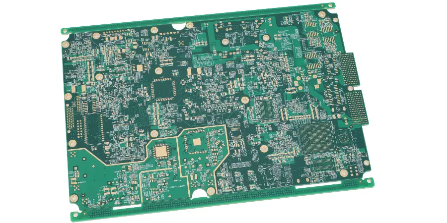
Summary: context, challenges, and benefits
Context: as data centers, 5G communications, automotive electronics, and industrial automation keep raising compute and reliability requirements, PCB are no longer just “component carriers”—they are the foundation of system performance. High density, high layer count, high frequency/high speed, and high power have become the norm, pushing PCB materials to new limits in heat resistance, electrical behavior, and long-term reliability.
Challenges: standard FR-4 (Tg ~130–140°C) can delaminate, blister (“popcorning”), and suffer uncontrolled Z-axis expansion leading to via cracking after repeated lead-free reflow (peak >250°C). Its dielectric performance also struggles to meet signal-integrity requirements above 10Gbps. Engineering teams must make tough tradeoffs among cost, performance, and manufacturability.
Benefits: this whitepaper-style high tg fr4 guide provides system and hardware engineers with a standardized material + stackup strategy. By adopting High Tg FR-4 (glass transition temperature Tg ≥ 170°C), PCB mechanical stability and reliability under high temperature improve significantly. We cover:
- Material-selection decisions: how to choose the most suitable High Tg material based on performance metrics.
- Stackup standardization: validated templates to accelerate design.
- Key-metric modeling: methods to predict impedance, thermal stress, and mechanical behavior.
- Manufacturing + validation loop: end-to-end quality control from incoming laminates to reliability testing.
The goal is to reduce design risk, shorten development cycles, and ensure excellent lifetime performance.
Tg (Glass Transition Temperature) is the critical temperature at which a polymer transitions from a hard “glassy” state to a softer “rubbery” state. High Tg FR-4 typically refers to epoxy laminates with Tg around 170°C and above. Above Tg, mechanical strength, dimensional stability, and electrical performance drop sharply. Choosing Tg well above both operating and processing temperatures is the first line of defense for PCB reliability.
Material decision tree: from metrics to applications
Choosing the right material is the starting point for stackup design. Based on years of volume-production data and failure-analysis experience, HILPCB’s materials lab summarizes the following decision tree to help you lock in target laminates quickly. This is a living pcb material whitepaper and will be updated as the market and technology evolve.
| Metric | Recommended material series (in stock at HILPCB) | Typical applications | Constraints & considerations |
|---|---|---|---|
| Baseline heat resistance (Tg ≥ 170°C) | ITEQ IT-180A, Shengyi S1000-2M | Server motherboards, industrial controllers, power modules, automotive ECU | Balanced performance at moderate cost. For >25Gbps signals, Df (loss) may become the bottleneck. |
| High-speed / low loss (Low Dk/Df) | ITEQ I-Speed, Panasonic Megtron 6 | 25/56/112Gbps backplanes, high-speed switches, optical modules, RF applications | Higher cost. Needs low-profile copper (VLP/HVLP) to fully realize loss benefits. Tighter lamination process window. |
| Halogen-free compliance (Halogen-Free) | Shengyi S1170G, ITEQ IT-170GRA | Consumer electronics, data centers, regulated medical devices | Belongs to halogen free pcb materials. Moisture absorption is often slightly higher than halogenated materials—requires stricter bake control. Dielectric performance is often better than same-class halogenated systems. |
| High voltage endurance / CAF resistance (High CTI/CAF) | ITEQ IT-180A, Isola 370HR | High-voltage power, inverters, BMS, dense BGA | CTI (Comparative Tracking Index) > 600V. CAF resistance is crucial for fine pitch + high bias designs. |
| Differential skew mitigation (Anti-Skew) | High-speed laminates using spread glass (e.g., 1067, 1086) | >10Gbps differential pairs (PCIe, Ethernet, USB) | Core strategy for glass weave skew mitigation. Spread glass reduces intra-pair delay mismatch caused by glass-weave pattern. Slight cost increase. |
| High thermal conductivity | Ventec VT-4B5, TUC TU-872SLK | LED lighting, power amplifiers, EV charging modules | Tc typically 1.0–3.0 W/m·K, far above standard FR-4 (~0.25 W/m·K). |
Stackup template library (Stackup Template Library)
Standardized stackups are key to predictable performance and efficient production. Below is HILPCB’s recommended general-purpose stackup template based on IT-180A (Dk ≈ 4.4 @1GHz), which you can use as a starting point.
Standard 6-layer stackup (S-GND-S-PWR-GND-S)
| Layer | Description | Material | Thickness (mm) | Dk/Df | Key usage |
|---|---|---|---|---|---|
| 1 | Signal 1 (Top) | Copper Foil | 0.018 (0.5oz) | - | High-speed signals / components |
| Dielectric | IT-180A (2116 PP) | 0.15 | 4.4/0.018 | Control top-layer impedance | |
| 2 | GND Plane | Core | 0.035 (1oz) | - | Primary reference plane |
| Dielectric | IT-180A Core | 0.76 | 4.4/0.018 | Core dielectric | |
| 3 | Signal 2 (Inner) | Core | 0.035 (1oz) | - | Inner signals (stripline) |
| 4 | Power Plane | Core | 0.035 (1oz) | - | Power plane |
| Dielectric | IT-180A Core | 0.76 | 4.4/0.018 | Core dielectric | |
| 5 | GND Plane | Core | 0.035 (1oz) | - | Primary reference plane |
| Dielectric | IT-180A (2116 PP) | 0.15 | 4.4/0.018 | Control bottom-layer impedance | |
| 6 | Signal 3 (Bottom) | Copper Foil | 0.018 (0.5oz) | - | Low-speed signals / components |
- Symmetry: stackup structure (copper thickness, dielectric thickness) should be symmetric about the center to prevent post-lamination warpage.
- Reference-plane continuity: high-speed signal paths must have continuous reference planes (GND or PWR) underneath to avoid impedance discontinuities and crosstalk.
- Core vs. prepreg (PP): prioritize core where possible—its dielectric thickness is more uniform and stable. PP thickness after lamination is affected by copper coverage.
Brief introduction to special stackup structures
- HDI: uses 1+N+1 or 2+N+2 with laser microvias (blind/buried) for higher routing density. Material selection must consider laser-drilling compatibility.
- Flex-Rigid: combines FR-4 rigid sections and polyimide (PI) flex sections for 3D interconnect; adhesion and CTE matching between materials are critical.
- MCPCB: combines FR-4 with aluminum/copper base to leverage high heat dissipation, for high-power LED and power conversion modules.
Modeling methods for impedance / thermal / mechanical metrics
Accurate modeling is the bridge between design intent and physical reality.
Impedance modeling (Impedance Modeling)
Impedance control is the core of high-speed design. Microstrip (outer layers) and stripline (inner layers) are the two most common transmission-line structures.
Microstrip impedance approximation:
Z₀ ≈ (87 / sqrt(Er + 1.41)) * ln(5.98 * H / (0.8 * W + T))Er: dielectric constant (Dk)H: dielectric thicknessW: trace widthT: copper thickness
Stripline impedance approximation:
Z₀ ≈ (60 / sqrt(Er)) * ln(1.9 * (2H + T) / (0.8 * W + T))
Key factors:
- Dielectric constant (Dk): intrinsic material property that varies with frequency. Use Dk at the target frequency.
- Dielectric thickness (H): actual post-lamination thickness matters. HILPCB uses Polar Si9000 and our
stackup strategydatabase for accurate simulation. - Trace geometry (W/T): etch accuracy affects final line width; include etch compensation.
- Solder mask: solder mask over outer traces has Dk (typically 3.0–3.5) and can reduce impedance by 2–3 Ω. This is a key
solder mask selection tutorialpoint and must be included for precision designs.
Thermal / mechanical metric modeling
- Coefficient of thermal expansion (CTE):
- X/Y CTE: High Tg FR-4 is typically 12–16 ppm/°C. Match CTE with large packages (BGA) to reduce solder-joint stress.
- Z-axis CTE: the most critical metric. Below Tg, CTE is ~40–60 ppm/°C; above Tg it can jump to >250 ppm/°C. Excess Z-CTE stretches via copper barrels during thermal cycling and causes fatigue cracks. A core benefit of High Tg materials is pushing this “knee” to a higher temperature so expansion stays low during soldering and operation.
- Decomposition temperature (Td): temperature at which material loses 5% weight. High Tg materials typically have Td > 340°C, providing sufficient lead-free process window.
- Delamination resistance (T260/T288 time): time a material can withstand 260°C/288°C without delaminating—critical for complex boards with multiple reflow passes.
Hybrid lamination / backdrill / special structures
To optimize cost vs. performance, advanced designs often adopt special structures.
Hybrid stack (Hybrid Stack)
Laminating different material types into a single PCB is the hybrid stack strategy.
- Scenario: a typical
Rogers-FR4hybrid uses low-loss Rogers (e.g., RO4350B) on the outer layers for RF, while inner digital/power layers use lower-cost High Tg FR-4. - Challenges:
- CTE mismatch: different materials may drive delamination or warpage.
- Lamination compatibility: temperature, pressure, and cure time must fit a process window compatible with all materials.
- Drilling parameters: differing hardness/resin content may require step drilling or optimized drill parameters. HILPCB enhances inter-material bonding via processes such as Plasma Desmear to ensure hybrid-board reliability.
Backdrill planning (Backdrill Planning)
backdrill planning guide is a key step for high-speed SI optimization.
- Principle: backdrilling removes unused via stub by drilling from the opposite side with a slightly larger bit than the original hole.
- Benefits: via stubs can form resonances that cause strong reflections and ISI. For >10–25Gbps links, removing stubs can significantly improve eye opening.
- Design considerations:
- Residual stub length: ideally <10 mil; requires precise backdrill depth control.
- Backdrill diameter: typically 8–10 mil larger than the original hole.
- Layer spacing: ensure sufficient safety distance between the backdrill stop layer and the next electrical layer.
Verification flow: from materials to reliability
A robust stackup strategy must include a closed-loop verification flow.
Incoming material inspection (IQC):
- DSC: measure Tg to confirm the laminate meets spec.
- TMA: measure CTE vs. temperature, especially Z-CTE.
Lamination process monitoring:
- monitor press temperature and pressure curves in real time to ensure every batch stays within the process window.
Impedance coupon testing:
- build standardized
coupon teststructures on each production panel. - use TDR to test coupons (often 100%) to keep single-ended and differential impedance within tolerance (typically ±10% or tighter ±7%).
- build standardized
Warpage measurement:
- after simulated reflow, measure bow & twist using projectors or laser-scanning tools to meet IPC-A-600.
Reliability testing:
- Thermal shock: rapid cycling between extremes (e.g., -40°C to 125°C) to evaluate via and solder-joint reliability.
- IST: quickly heat/cool test coupons to emulate repeated soldering stress while monitoring via resistance changes—an efficient method to evaluate interconnect reliability.
- Micro-section: the final “judge”—inspect via copper quality, lamination structure, delamination, and cracks under microscope.
DFM/DFR checklist
This checklist merges manufacturability (DFM) and reliability (DFR) rules—35+ items—to help you avoid common pitfalls during design.
| Category | Rule | Recommended parameter / note | Verification method |
|---|---|---|---|
| Material selection | Tg choice | Tg should be 20–25°C higher than max operating/soldering temperature | Datasheet, IQC (DSC) |
| Dk/Df consistency | Choose materials with low Dk/Df variation across frequency and lots | Datasheet, VNA test | |
| CTI grade | Select based on working voltage; high-voltage apps > 600V | UL yellow card, datasheet | |
| Halogen-free | Confirm IEC 61249-2-21 compliance | Datasheet | |
| Stackup design | Symmetry | Stackup should be symmetric about center | Design review, CAM |
| Copper balance | Keep copper distribution balanced; avoid large open areas | Design review, CAM | |
| PP resin flow | Select PP resin flow based on copper coverage | Simulation, production data | |
| Prefer core | Prefer core dielectric between key impedance layers | Design review | |
| Impedance control | Impedance tolerance | Standard ±10%; high-speed ±7% or ±5% | Spec, TDR |
| Continuous reference plane | No splits/slots under impedance traces | DRC, manual review | |
| Solder-mask impact | Include solder mask in impedance simulation | Simulation tools (Polar) | |
| Copper roughness | >10GHz designs must consider copper roughness loss | Material selection (VLP/HVLP) | |
| Vias & drilling | Aspect ratio | Through vias < 10:1; HDI microvias < 1:1 | Design review, DFM |
| Via-in-pad | Resin plug + copper fill/planarization process | Process spec | |
| Backdrill stub length | < 10 mil (0.254mm) | Spec, TDR/micro-section | |
| Non-functional pads (NFP) | Remove inner-layer NFP to reduce via capacitance | CAM auto-optimization | |
| Thermal management | Thermal vias | Array under heat sources, connect to heat-spreading planes | Design review |
| Z-CTE | Choose material with Z-CTE (α2) < 300 ppm/°C | Datasheet, IQC (TMA) | |
| Td | Td > 340°C for lead-free | Datasheet | |
| Signal integrity | Glass weave effect | Use spread glass for >10Gbps differential pairs | Material selection |
| Intra-pair matching | Length mismatch < 5 mil | EDA constraints | |
| Avoid right angles | Use 45° or arcs | DRC | |
| Surface finish | surface finish comparison |
ENIG for high frequency/BGA; OSP lower cost but narrow solderability window | Select per application |
| Gold thickness | ENIG Au 1–3 u" | Process spec, XRF | |
| Solder mask | solder mask selection tutorial |
LPI is mainstream; color slightly affects impedance | Process spec |
| Solder dam | Keep dam between fine-pitch pads to prevent bridging | DFM check (≥ 4 mil) | |
| Mask opening | Use NSMD for BGA pads | Design review | |
| Reliability (DFR) | CAF prevention | Maintain spacing vs. CAF capability | DFM check |
| Pad design | BGA pad size/shape per IPC-7351 | Design review | |
| Teardrops | Add teardrops to improve vibration robustness | CAM auto-add | |
| Edge clearance | Keep copper/components away from V-cut/stamp holes | DFM check (≥ 0.5mm) | |
| Gold finger chamfer | 30° or 45° chamfer for insertion | Process spec | |
| Testability (DFT) | Reserve test points on key nets | Design review | |
| Silkscreen clarity | Silkscreen must not cover pads; keep adequate height/width | DFM check | |
| Mask thickness | Typical solder mask thickness over copper: 0.5–1.2 mil | Process spec |
HILPCB closed-loop services + CTA
Creating a comprehensive high tg fr4 guide is only step one. The real challenge is executing it precisely at every production step. HILPCB provides more than PCB fabrication—we deliver a complete material + stackup strategy solution.
- Broad material stock: dozens of High Tg and high-speed materials from ITEQ, Shengyi, Panasonic, etc., to avoid schedule waiting and enable flexible substitutions.
- Professional stackup simulation: our engineers use Polar Si9000 and other industry-standard tools to provide free stackup design and impedance simulation—optimizing upfront.
- Advanced lab capability: in-house lab with DSC, TMA, TDR, XRF, and micro-section equipment to monitor and validate key parameters from incoming materials to finished boards.
- DFM driven by production data: our DFM engine integrates millions of production records to identify manufacturability and reliability risks before production and provide optimization suggestions.
We know that a reliable stackup design is the foundation of product success.
Is your next high-reliability project facing material selection or stackup design challenges? Contact HILPCB materials experts now to get a free stackup review and material-selection recommendations. Let our expertise and full-process quality control help your project succeed from the start.
Conclusion
In summary, this article uses high tg fr4 guide to deliver a material-selection decision tree, stackup templates, impedance/thermal modeling methods, and a closed-loop manufacturing verification flow—plus a DFM/DFT/DFR checklist—to help engineering teams standardize stack design and systematically control risk across design, materials, and testing. By following these checklists and process windows, and involving HILPCB’s DFM/DFA team early, you can accelerate prototype and volume delivery while maintaining quality and compliance.
If you need fabrication/assembly support, contact HILPCB via Turnkey Assembly or SMT Assembly to get DFM/DFT suggestions.
Common Questions
What problem does High Tg FR-4 solve compared with standard FR-4?
High Tg FR-4 improves mechanical stability and reliability when boards face high assembly temperatures, repeated reflow, and elevated operating heat. It reduces the risk of delamination, excessive Z-axis expansion, and via-related failure.
Does choosing High Tg FR-4 automatically make a board suitable for high-speed design?
Not automatically. Tg improves thermal robustness, but signal integrity at very high data rates also depends on Dk, Df, copper profile, glass weave, and stackup execution. Material selection must match both thermal and electrical requirements.
When should engineers consider halogen-free or anti-skew variants in a High Tg stackup?
Halogen-free materials matter when environmental compliance or customer requirements demand them, while anti-skew options help for sensitive differential pairs above high data rates. These variants are chosen based on project constraints, not just as defaults.
What should be verified before volume production of a High Tg FR-4 design?
Teams should verify laminate choice, stackup thickness control, impedance behavior, thermal reliability, and moisture or reflow robustness. A closed-loop process usually includes incoming material control, coupons, and reliability validation.