
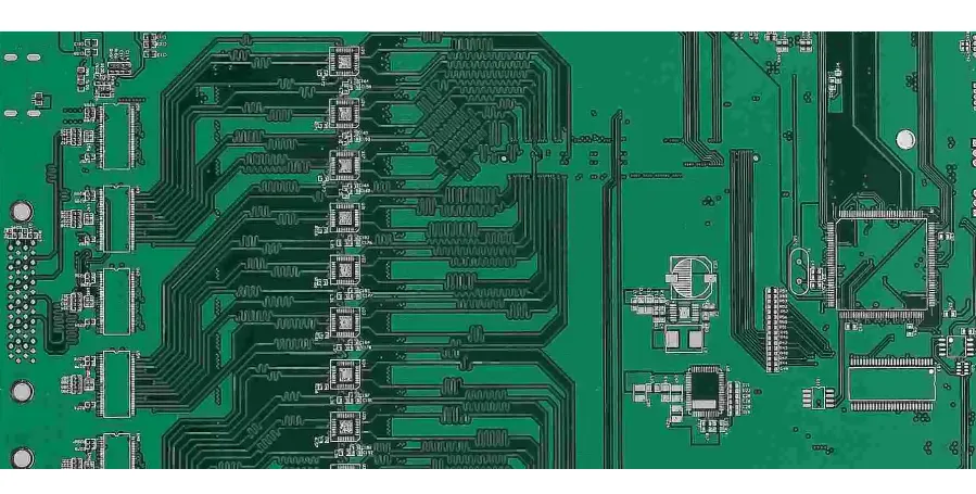
Controlled impedance matters when a routed connection must behave as a transmission line for the signal’s edge rate, length and interface requirements. Specify the target, reference plane, geometry and fabrication tolerance before release. It reduces one source of reflection risk; loss, crosstalk, terminations and receiver timing still need channel verification.
Understanding Controlled Impedance and Why It's Essential
A controlled impedance PCB uses defined conductor and dielectric geometry to meet specified characteristic-impedance limits for selected nets. This is not a DC resistance measurement. Discontinuities can reflect signal energy; attenuation also depends on conductor and dielectric loss, so impedance control alone does not establish link margin or EMC compliance.
At HilPCB PCB Factory, we understand that impedance controlled PCBs are crucial in:
- RF and microwave circuits
- Gigabit Ethernet systems
- DDR4 and DDR5 memory routing
- High-speed serial communication like USB, HDMI, PCIe, and DisplayPort
Impedance mismatches can cause signal reflections, degrade performance, and trigger data errors, making precise control essential.
How is PCB Impedance Calculated and Controlled?
Precise impedance control begins with accurate PCB impedance calculations. Impedance calculation depends on several key variables:
- Material grade, glass/resin construction and a suitable design Dk at stated frequency/method
- Finished trace width, etched cross-section and conductor thickness
- Pair spacing where applicable, dielectric thickness and reference-plane geometry
- Solder mask for outer layers, copper roughness and transitions where relevant; copper weight in oz/ft² is an areal mass, so use the actual finished thickness in the model
Use a field solver or a model suitable for the actual microstrip/stripline structure. Agree available material constructions and finished geometry with the fabricator, including etch and pressing tolerances, before routing critical nets.
Examples with Defined Interface Scope
| Signal Standard | Typical Impedance | Structure Used |
|---|---|---|
| TI DP83867 1000BASE-T MDI example | 100 Ω differential | PHY-to-magnetics routing; follow the device layout guide |
| TI AM57xx/DRA7xx USB3.0 SuperSpeed example | 90 Ω differential nominal | Table A-2 platform target; confirm the selected device and interface revision |
| TI AM57xx/DRA7xx HDMI TMDS example | 100 Ω differential nominal | Table A-2 platform target; do not apply unchanged to every HDMI mode |
| DDR4/DDR5 | Interface- and platform-specific impedance targets | Reference the memory-controller and JEDEC board design guide |
The numerical examples are supported by TI SPRAAR7J, Table A-2 and the DP83867 datasheet, MDI layout section. They are not a universal tolerance list or bare-board acceptance specification. The selected controller and interface requirements govern the actual release.
The Impedance Calculator provides a preliminary estimate from entered stackup parameters. Confirm its model assumptions, geometry and Dk; a calculator result does not replace fabrication review or a representative coupon measurement. Laser microvias or sequential lamination are options only where the selected construction needs them.
HilPCB PCB Factory Specializes in Complex and Special Material Designs
For complex stacks and special materials, specify the named grade, copper, bonding system, layer geometry and qualification evidence. Material families that may be considered include:
- High-frequency laminates (Rogers, Taconic, Nelco)
- High-Tg FR4 and hybrid FR4 stackups
- Flexible and rigid-flex substrates for complex shapes and dynamic applications
- Ceramic or insulated-metal constructions where thermal, dielectric and routing requirements justify them; these are not interchangeable with a multilayer RF laminate
Our PCB products, including FR4 PCB and HDI PCB, identify construction options. Confirm the actual supplying site, available material combination and offered scope; a product listing is not evidence that every stackup is qualified.
Beyond Controlled Impedance – Comprehensive PCB Manufacturing Services
HILPCB provides controlled-impedance fabrication and assembly with advanced modeling, laser microvias, sequential lamination and dielectric-thickness control options. Available materials and constructions include Rogers, Taconic, Nelco, high-Tg and hybrid FR-4, flex/rigid-flex, ceramic and aluminum routes when suitable. Services include quick-turn prototypes, turnkey/kitting, DFM and stackup optimization, layout and manufacturing consultation, TDR/AOI and other scoped testing, process visibility and prototype-to-volume support. Convenient payment and global-logistics support remain available. Confirm the actual material combination, quoted schedule, measurement method and production records for the order.
Our factory is equipped with automated impedance verification tools (TDR), AOI inspection, and advanced test capabilities.
A fabrication or assembly enquiry can include the following work, with scope and records agreed for the actual order:
- Prototype quantity and requested schedule, subject to material and process availability
- Defined turnkey assembly/kitting with approved sources and substitution control
- DFM review, stackup agreement and disposition of geometry changes affecting impedance
- Convenient payment and global logistics support
- Engineering communication on critical nets, target/tolerance, test method and construction changes
Agree coupon geometry, reference construction, TDR calibration/rise time, fixtures, measured region, sampling and acceptance limits. Retain the results against the released revision. AOI checks visible manufacturing features; it is not an impedance measurement, and a passing coupon does not by itself prove complete-channel loss or timing.
Partner with HilPCB PCB Factory for Reliable Impedance Controlled PCBs
For a HILPCB quotation, provide the stackup, approved material construction, critical-net impedance schedule, conductor geometry, reference layers and required test records. Resolve manufacturing adjustments with the design authority before release and preserve the approved baseline through production.
Compare offered capability and evidence against those inputs. Manufacturing acceptance supports the defined board construction; verify connectors, vias, packages, terminations and active-device behavior as part of the complete channel.