
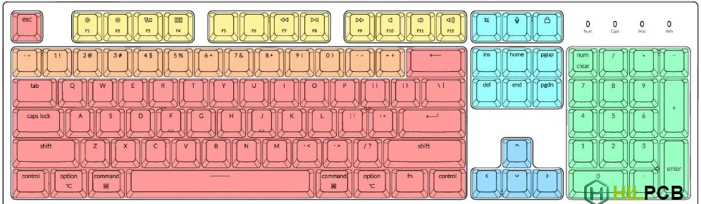
The layout phase transforms your keyboard PCB design schematic into a physical board that can be manufactured and assembled. Component placement determines not only electrical functionality but also mechanical compatibility with cases, plates, switches, and keycaps. Precise positioning is critical—a switch hole misaligned by even 0.5mm can cause binding or prevent insertion.
HILPCB fabricates keyboard PCBs with the registration accuracy required for proper switch alignment and reliable hot-swap socket operation across all standard manufacturing tolerances.
In This Guide
- Keyboard Unit Spacing System
- Switch Footprint Specifications
- Hot-Swap Socket Integration
- Stabilizer Positioning
- MCU and Component Placement
- RGB LED Layout
- Layer Organization and Routing Strategy
Keyboard Unit Spacing System
Before placing any components, understanding the keyboard unit system is essential. This standardized spacing defines key positions across all layouts worldwide, ensuring compatibility between PCBs, plates, cases, and keycap sets from different manufacturers.
Standard keyboard spacing follows a 19.05mm (0.75 inch) grid known as "1u" spacing. Switch center points are placed exactly on this grid, with keycaps overhanging symmetrically. This universal standard originated in the typewriter era and remains absolute—deviation results in incompatibility with the vast ecosystem of keyboard components.
Key widths expressed in units:
- 1u (19.05mm): Standard alphanumeric keys
- 1.25u (23.81mm): Bottom row modifiers (Ctrl, Alt, Win)
- 1.5u (28.58mm): Tab, Backslash
- 1.75u (33.34mm): Caps Lock
- 2u (38.1mm): Numpad 0, optional Backspace
- 2.25u (42.86mm): Left Shift, Enter
- 2.75u (52.39mm): Right Shift
- 6.25u (119.06mm): Standard spacebar
- 7u (133.35mm): Alternative spacebar
Layout Design Tools
Keyboard Layout Editor (KLE) at keyboard-layout-editor.com provides a web-based interface for designing and visualizing layouts. It exports JSON data compatible with various PCB tools and includes a community library of existing layouts as starting points.
ai03 Plate Generator converts KLE data into DXF files for plate manufacturing and—more relevant for PCB designers—provides exact switch position coordinates. These can be imported into KiCad, Altium Designer, Eagle, or other EDA tools to ensure precise switch placement.
KiCad keyboard libraries (ai03, foostan, keebio) provide pre-made switch footprints with correct dimensions. Using established libraries prevents dimensional errors that would require complete board redesign.
Switch Footprint Specifications
Cherry MX-compatible footprints dominate custom keyboards, supported by switches from Cherry, Gateron, Kailh, Durock, JWK, Tecsee, and dozens of other manufacturers. Understanding exact specifications prevents costly errors.
Critical Dimensions (Non-Negotiable)
- Center Hole: 4.0mm diameter for switch housing alignment
- Metal Pin Holes: 1.27mm diameter at 6.35mm horizontal spacing from center
- Pin Positions: Precisely per Cherry MX datasheet—even 0.1mm deviation causes insertion problems
Optional Features
- PCB-Mount Pin Holes: 1.7mm diameter for 5-pin switch plastic alignment legs—enables plateless builds
- LED Slot: 1mm × 4mm rectangular cutout for through-hole LEDs (traditional approach)
- SMD LED Pads: North or south of switch center for modern addressable RGB
Universal Footprint Strategy
Designing footprints supporting multiple configurations maximizes build flexibility and market appeal for group buy projects. A universal footprint includes: MX switch pin holes (required), PCB-mount pin holes (optional for builders), through-hole LED slot (traditional compatibility), SMD LED pads (modern RGB), hot-swap socket pads (tool-free switch changes), and diode pads (both SMD and through-hole options).
This approach allows one PCB design to support soldered builds, hot-swap builds, various LED options, and plate-mounted or plateless construction.
Kailh Hot-Swap Socket Specifications
Hot-Swap Socket Integration
Hot-swap sockets enable switch replacement without soldering—essential for enthusiast keyboards where users experiment with different switches. The additional complexity and cost are justified by dramatically improved user experience.
Kailh Hot-Swap Sockets
Kailh sockets are the dominant choice, mounting on the PCB bottom via surface-mount pads. Each socket measures 7.4mm × 3.3mm and sits 1.8mm below the PCB surface when installed. This clearance requirement is critical—verify adequate case depth before committing to hot-swap design.
Pad specifications: 2.55mm × 2.55mm square pads at 6.35mm center-to-center spacing, matching switch pin positions exactly. Insufficient pad size causes weak solder joints that fail during switch insertion; excessive size wastes board space without benefit.
Layout considerations: Maintain clear areas where socket bodies sit (no traces or vias beneath sockets), keep consistent socket orientation throughout for uniform appearance, and ensure adequate copper for solder joint strength—1oz copper is typically sufficient, but proper pad design matters more than copper weight.
Mill-Max Socket Alternative
Mill-Max sockets (0305 and 7305 series) provide hot-swap capability with standard switch footprints. These cylindrical sockets install into through-holes, gripping switch pins through spring-loaded internal contacts.
Key advantage: Compatible with existing non-hotswap PCB designs—enables retrofitting or designing boards that support both soldered and hot-swap builds without separate footprints.
Requirements: Enlarged pin holes (3.30mm for 0305 series vs standard 1.27mm). Because sockets sit within PCB thickness rather than below, there are no bottom clearance concerns.
Trade-off: Higher per-socket cost than Kailh, but design flexibility may justify the premium for certain applications.
Stabilizer Positioning
Keys 2u and larger require stabilizers for balanced actuation—without stabilizers, pressing the edge of wide keys causes tilting and inconsistent feel. Cherry-style PCB-mount stabilizers are standard for custom keyboards.
Housing Hole Dimensions
- Housing holes: 3.0mm diameter
- Wire clearance slots: Sized for free wire movement
Stabilizer Spacing by Key Width
The distance between stabilizer housing centers varies by key width:
- 2u through 2.75u keys: 23.8mm spacing (11.9mm each side from switch center)
- 6.25u spacebar: 100mm spacing (50mm each side from switch center)
- 7u spacebar: 114.3mm spacing (57.15mm each side)
These dimensions are standardized across Cherry-style stabilizers from all manufacturers. Costar and other stabilizer types have different requirements and are less common in custom designs.
Screw-In Stabilizer Support
Screw-in stabilizers provide more secure mounting than clip-in variants, reducing rattle and improving long-term stability. They require additional M2 screw holes:
- Hole size: 2.2mm diameter, non-plated (NPTH)
- Position: 0.5mm toward key center from each housing hole
- Note: Verify screw holes don't cut through bottom-layer traces during layout
Most enthusiast keyboards include screw-in support even when shipping with clip-in stabilizers—giving users upgrade options.
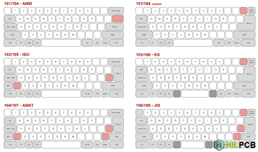
MCU and Component Placement
Beyond switches, keyboard PCBs contain the microcontroller, passive components, USB connector, ESD protection, and optionally RGB drivers. Strategic placement simplifies routing and improves manufacturability.
MCU Positioning
Edge placement near the USB connector minimizes critical USB trace length—the most common approach for 60% and TKL layouts. Short USB traces improve signal integrity and simplify controlled-impedance routing.
Center placement equalizes matrix trace lengths to all switch positions, potentially beneficial for signal timing consistency in large keyboards. However, center placement often conflicts with spacebar stabilizers on common layouts.
Daughterboard designs provide MCU placement flexibility since USB routing goes to the JST connector rather than directly to USB-C.
Passive Component Guidelines
- Decoupling capacitors: Within 3mm of MCU VCC pins—closer is always better. These filter high-frequency noise; effectiveness decreases rapidly with distance.
- USB series resistors (22Ω): Close to MCU with short traces to USB pads
- ESD protection: At the USB connector, not near MCU—protection must intercept transients before they propagate
- Crystal/resonator: Within 10mm of MCU oscillator pins, away from high-speed digital signals
Diode Placement Strategies
Each switch requires an associated diode. Common approaches:
- Adjacent to switch: On top layer near switch—simplifies hand soldering and visual inspection
- Under switch: SMD diode on bottom layer beneath switch—hidden when assembled, frees top surface for LEDs
- Integrated in footprint: Small SMD (SOD-323) between switch pins—maximum space efficiency
Whichever approach, orientation must be consistent throughout. Mixed orientations cause matrix malfunction. See keyboard diode direction.
Recommended Design Rules for Keyboards
RGB LED Layout
Per-key RGB requires LED placement at each switch position with data lines following the LED chain sequence.
LED Orientation Options
South-facing LEDs (below switch center) ensure compatibility with all keycap profiles including Cherry—the preferred orientation for maximum compatibility. Some switch/keycap combinations experience interference with north-facing LEDs.
North-facing LEDs (above switch center) provide better legend illumination on top-printed keycaps. Choose this if targeting specific compatible switch/keycap combinations.
Underglow LEDs mount on PCB bottom around the perimeter, illuminating beneath the keyboard. Space evenly for uniform glow, orient data-in pins consistently for simple chain routing.
Data Chain Routing
WS2812B/SK6812 LEDs use serial protocol—data cascades through the chain. Physical routing must follow the logical sequence: LED1 data-out → LED2 data-in → LED2 data-out → LED3 data-in, etc.
Plan the chain before other routing. Serpentine pattern works well: Row 1 left-to-right, Row 2 right-to-left, alternating—minimizes trace length while creating intuitive firmware addressing.
Layer Organization and Routing Strategy
Most keyboard PCBs use 2-layer construction—sufficient for typical designs while maintaining low cost and broad manufacturer compatibility.
Layer Assignment Strategy
Top Layer: Switch pads and footprints, row traces (horizontal direction), MCU and USB connector, passive components
Bottom Layer: Column traces (vertical direction), ground copper fill in unused areas, hot-swap socket pads, SMD diodes (if under-switch placement)
This organization minimizes vias by keeping horizontal and vertical routing on separate layers. Row traces connect horizontally without layer changes; column traces via down once per switch position and route vertically.
Design Rules for Cost-Effective Manufacturing
Keyboard PCBs don't require aggressive design rules. Conservative rules reduce cost and improve yield:
- Trace/Space: 6/6mil (0.15mm) is comfortable and standard-priced. 8/8mil provides extra margin.
- Via Drill: 0.3mm standard, adequate for keyboard routing density
- Via Pad: 0.6mm minimum for reliable annular ring
Note: While HILPCB supports 2/2mil (50μm) trace/space for high-density applications, standard keyboards should use 6/6mil or larger—finer rules increase manufacturing cost without benefiting typical keyboard designs.
Routing strategies detailed in keyboard PCB trace routing.
HILPCB Layout Fabrication
HILPCB provides precision fabrication for keyboard layouts with capabilities supporting both standard and advanced designs:
- Registration Accuracy: Layer-to-layer alignment within ±50μm for reliable switch alignment
- Hole Placement: Consistent positioning for proper switch insertion
- Standard Design Rules: 6/6mil trace/space at standard pricing
- Advanced Capability: 2/2mil available when designs require (HDI, dense MCU breakout)
- Surface Finishes: ENIG for hot-swap durability, multiple mask colors
SMT assembly services handle diodes, MCU, passives, and hot-swap socket installation with verified component orientation.
Submit your layout for fabrication review—our team verifies alignment and manufacturability before production.