
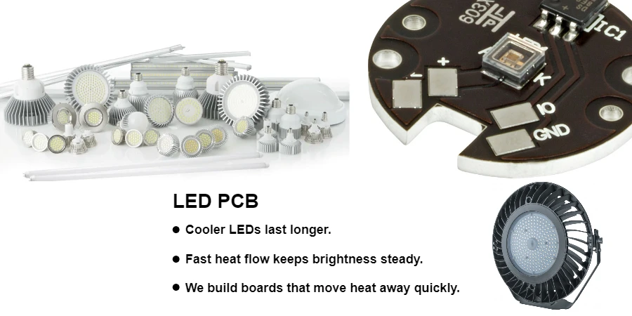
An LED board's thermal performance depends on the complete path from the junction through its package, solder, PCB, interface material and heat sink to the surrounding air. A metal base can spread heat well while a thin insulating layer or poor mounting interface remains the bottleneck. Start with the actual LED, drive conditions, ambient temperature and fixture construction before selecting a material by its conductivity alone.
HILPCB manufactures metal-core PCBs, ceramic PCBs and thermal PCB constructions, with modeling, assembly and test options. These routes also serve power conversion, motor drives, RF amplifiers and other electronics. The useful choice is the construction that meets the project's thermal, insulation, routing and assembly requirements together.
Why LED Heat Dissipation Matters
Junction temperature affects light output, color, electrical characteristics and degradation. Use the selected device's operating limits and lumen-maintenance information at the intended current and temperature. A temperature used for optical binning is not automatically a maximum operating limit, and no universal “10°C rise halves life” rule establishes fixture life.
For a heat-flow model, the heat generated is electrical input minus radiant optical output. Lumens are photometric units and cannot simply be subtracted from electrical watts. Driver losses and optical power absorbed elsewhere in the fixture add other heat sources. Also check the power convention of any published thermal resistance before applying this model: some LED thermal-characterization values are normalized to electrical input rather than heat alone.
Selecting PCB Materials for the Thermal Path
FR-4 with copper spreading and vias: FR-4 can be suitable for lower loads or a well-engineered path into a chassis or heat sink. Copper area, via construction, soldering and board geometry affect the result. Do not reject every LED application merely because the laminate's bulk conductivity is low.
Aluminum MCPCB: An insulated metal substrate combines circuit copper, a dielectric and a metal base. HILPCB's metal-core route lists aluminum 5052/6061, with 0.8–2.0 mm standard board-thickness options and 0.5–3.2 mm under advanced review. Dielectric constructions commonly use 1–3 W/m·K materials; the route lists advanced options up to 8 W/m·K, subject to the selected material datasheet and construction review. These are material/construction choices, not an effective conductivity guaranteed through the complete board. The base spreads heat; the fixture still needs enough surface area or another heat-rejection path.
The same route lists 75–150 µm standard dielectric and ≤50 µm advanced options. For a simple one-dimensional illustration, a 100 µm dielectric with assumed conductivity 2 W/m·K across 25 mm² gives R = t/(kA) = 2 K/W. At 5 W through that area, the layer alone adds 10 K. Halving thickness would halve that ideal layer resistance, but insulation requirements, manufacturability, spreading and the other interfaces still need review. This calculation is not a finished-board rating.
Ceramic substrates: HILPCB's ceramic route lists alumina material options at 24–30 W/m·K and advanced AlN options at 170–190 W/m·K, with DBC/DPC constructions. Confirm the grade, measurement conditions, metallization and thickness for the actual order. Ceramic can suit compact high-flux modules, UV systems and packaged COB assemblies, but material conductivity alone does not predict the LED junction temperature. CTE, mechanical support and solder stress also affect the selection.
Copper-core and heavy-copper boards: The metal-core route includes copper C110, while heavy copper PCB construction can improve lateral spreading and current distribution. Choose the copper cross-section, insulation and interfaces together. A bulk-metal conductivity value is not the effective thermal conductivity of a multilayer assembly, nor is copper weight a complete current rating.
Thermal Vias, Copper and Heat-Sink Integration
Thermal vias: On a suitable FR-4 or multilayer construction, plated or copper-filled vias can connect a thermal land to lower copper regions. Hole count, diameter and pitch follow the LED land, board thickness, plating/fill process and soldering requirements. HILPCB's thermal route lists reference arrays around Ø0.30–0.50 mm on 1.0–1.5 mm pitch; these are review inputs rather than a universal optimum. A smaller device may not accommodate such an array.
Open holes beneath a soldered thermal pad can draw solder away from the joint. Agree via-in-pad filling/capping or another validated solder-control method with the assembler. A resin-filled via is not thermally equivalent to a copper-filled via. On a metal-core board, do not extend conductive vias into an electrically isolated metal base without an engineered insulation/construction scheme. Stacked microvias are an advanced multilayer/HDI option, not a necessary cooling feature for every LED board.
Copper pours: More copper may help spread heat or reduce voltage drop, but it also changes etching and reflow behavior. Select copper weight and thermal-relief connections with trace clearance, current, solderability and the thermal model. There is no universal 2 oz minimum or copper-grid pattern that guarantees both low warpage and good heat flow.
Heat-sink and TIM interfaces: Surface flatness, interface thickness, pressure and mounting all affect contact resistance. A TIM fills small gaps but also adds its own thermal resistance; excess thickness can defeat a conductivity upgrade. Define mounting holes, torque/pressure limits and the intended contact area without overstressing the PCB or ceramic. A heat pipe or vapor chamber can be part of the external thermal assembly when justified; embedding one in a PCB is a specialized construction to assess separately.
Placement and cooling: Allow for thermal interaction between adjacent LEDs and driver components. Board-edge placement does not automatically improve cooling: airflow, heat-sink orientation, enclosure and hot neighboring parts determine the result. Review the installed configuration, including fan failure or blocked airflow where those are specified operating cases.
Thermal Calculation and Validation
For an illustrative single-source, steady-state model using heat-normalized resistance:
Tj ≈ Ta + Pheat × Rtotal
Assume one emitter receives 10 W electrical input and emits 3 W radiant optical power, leaving 7 W heat. With assumed junction-to-ambient resistance 8 K/W and ambient 40°C, the estimate is 96°C. If the project's chosen junction-temperature target were 105°C, the total resistance budget would be (105 − 40)/7 ≈ 9.29 K/W. This target is an example, not a universal LED limit; leave margin for tolerances and measurement uncertainty. An array with shared spreading and mutual heating needs an appropriate multi-source model.
Match every resistance to its defined reference point and power basis. Lumileds WP23 explains an electrical-input basis for its stated device values and distinguishes junction-to-case from junction-to-Ts characterization. Its Ts reference may not lie directly in the heat path. Applying a heat-only power value to an electrically normalized resistance can underestimate temperature. Use the selected LED's actual datasheet/application method rather than adding incompatible coefficients into a chain.
Thermal simulation: FEA can compare dielectric thickness, copper distribution, interfaces and mechanical stress; a model that includes airflow needs suitable convection/flow conditions. Include actual mounting, material properties, heat sources and duty cycle. Transient models help assess warm-up and cycling, but require representative boundary conditions and correlation with a prototype.
Temperature measurements: IR imaging locates surface hot spots; it does not directly measure a covered LED junction. Emissivity and reflections can distort absolute results. Place thermocouples at the manufacturer's specified reference location and control attachment and optical heating effects. Cree LED's thermal guide, in its measurement sections, discusses realistic installation conditions, stabilization and these measurement limitations.
Record ambient, drive current/voltage, optical-power assumption or method, sensor location, airflow, enclosure, TIM and mounting. Compare the same configuration with the model. Thermal cycling or accelerated aging can support a defined qualification plan; a test duration alone cannot demonstrate a particular field lifetime without a justified model and acceptance criteria.
Application-Specific Thermal Choices
Automotive headlights: A compact array can combine high local heat flux with restricted cooling. Review package data, shared heat spreading, mounting and the actual qualification profile. PCB construction supports that design; it does not establish a vehicle service-life promise.
Horticultural luminaires: Long duty cycles and greenhouse moisture make heat rejection, sealing, connector access and serviceability important. If liquid cooling is proposed, include the mechanical interfaces, leak-risk controls and separate validation rather than assuming an aluminum board is itself water-cooled or sealed.
UV and UV-C systems: Package materials, wavelength, optical exposure and heat flux influence the construction. Ceramic/DBC can be a candidate, while sensing or active cooling may be needed for the actual temperature target. Germicidal or medical-product efficacy and safety require their own verification.
Stadium and stage-lighting retrofits: Modular LED boards can simplify replacement, but the connector, current distribution, heat-sink contact and optics must remain compatible. Define actual module power and channel currents, then test uniformity and temperature at representative installation conditions. Module power does not determine current without its operating voltage, and test duration alone does not establish service life.
Thermal Engineering, Fabrication and Assembly with HILPCB
HILPCB's metal-core, high-thermal and ceramic routes include material/process review and FEA-based modeling options. The high-thermal service lists IR imaging, thermal-resistance and cycling test options; the specific specimen, method, limits and records belong in the order. Its construction choices include thermal-via processes and TIM pre-application. Turnkey assembly connects sourcing and board assembly, while box build can include heat sinks, enclosure integration and defined system tests.
Send the LED part number and application data, drive/current or duty-cycle requirements, allowable temperatures, ambient/airflow conditions, fabrication and assembly files, quantities and the enclosure/heat-sink drawing. Identify dielectric/insulation requirements, thermal-pad/via construction, TIM and mounting constraints. For a replacement module, include connector, optical and service-fit requirements as well.
Use the review to compare a conventional via-based board, MCPCB or ceramic route against the same thermal budget. Agree which work covers modeling, first-article assembly, temperature correlation and any reliability tests, so the quotation separates tooling and validation from recurring production. For wider thermal designs, include the power electronics, RF amplifier or computing heat sources that share the assembly.
For application-specific thermal builds, HILPCB can review integrated mounting, heat-pipe or vapor-chamber constructions, water-cooling layouts, sealed connectors and temperature monitoring, then plan thermocouple measurements, correlated thermal data and accelerated testing. These options are assessed against the assembly, enclosure, operating profile and agreed test method; the results describe the tested configuration and do not establish a universal LED lifetime or efficiency.
Frequently Asked Questions
What is the best PCB material for LED heat dissipation?
Choose from the thermal and insulation budget. FR-4 with suitable copper/vias, aluminum or copper MCPCB, and ceramic each solve different constraints. Compare the complete heat path, thickness, assembly, mounting and cost; a 2–3 W/m·K dielectric is not automatically the best choice for every LED.
How many thermal vias should I use under each LED?
Use the package land pattern and validated via/assembly construction. There is no universal 9–16-hole array. Check available pad area, finished hole/plating, solder wicking, fill/cap, electrical isolation and the path to the sink. Compare candidates by thermal analysis and representative measurements.
Can HILPCB manufacture boards for non-LED thermal applications?
Yes. Its thermal, metal-core, ceramic and heavy-copper routes also support power conversion, motor-drive and RF/power modules. Provide the actual heat sources, insulation and assembly conditions to select a construction and test scope.
What thermal simulation services are available?
The thermal and ceramic services include FEA-based heat/stress modeling. Define geometry, material data, interfaces, loads and ambient/cooling conditions, together with the required outputs. Junction estimation must follow the actual package's reference points and power convention; prototype correlation remains part of validation.
How can thermal performance be validated?
Specify IR or thermocouple locations and conditions, any package-specific junction-estimation method, thermal-resistance measurement and required cycling/aging. HILPCB's listed thermal test options can be scoped for the order; agree samples, acceptance and records rather than assuming every production board receives full lifetime testing.