
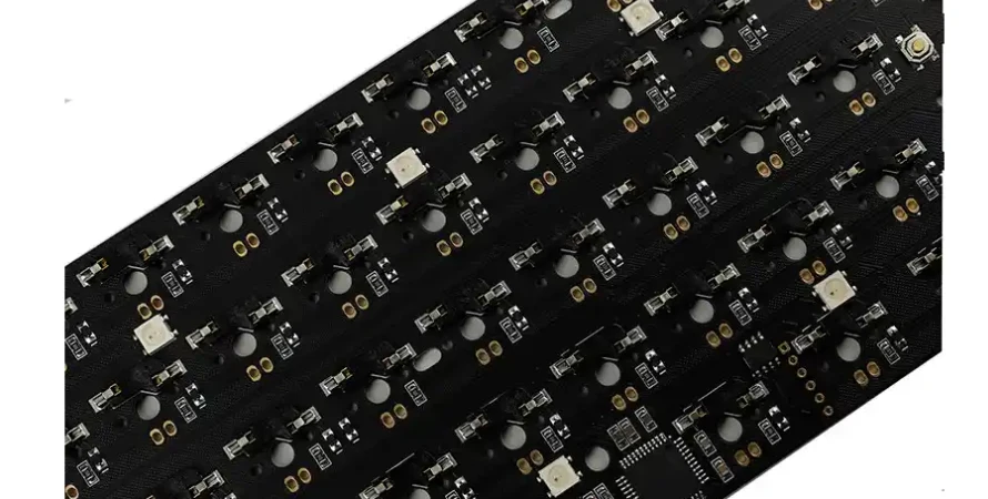
While standard 2-layer PCBs serve many keyboard applications effectively, advanced designs increasingly require Multi-Layer PCB for Keyboards to achieve their performance goals. Wireless connectivity, sophisticated RGB implementations, and compact form factors create routing and signal integrity challenges that additional layers elegantly solve. Understanding when multi-layer construction is necessary—and when it isn't—helps designers make cost-effective decisions.
This technical guide explores multi-layer PCB applications in keyboard design, covering architecture decisions, layer assignment strategies, and practical implementation considerations.
Menu Navigation
- Wireless, RGB, and Compact Layouts: When You Need More Layers
- 4-Layer Stack-Up Design and Layer Assignment Strategy
- 6-Layer PCB for Premium Wireless and Multi-Function Keyboards
- Signal Integrity, EMC, and Power Distribution Benefits
- Multi-Layer PCB Cost vs Performance Trade-offs
Wireless, RGB, and Compact Layouts: When You Need More Layers
Multi-layer PCBs solve specific design challenges, but their additional cost requires justification. Understanding the triggers helps make appropriate technology selections.
1. Wireless Keyboard Requirements
Wireless designs frequently require 4+ layers for optimal performance. RF circuits need controlled impedance traces with solid reference planes. Antenna performance depends on proper ground plane geometry. Battery management circuits benefit from isolated power layers. Wireless Keyboard PCB designs achieve best performance with dedicated layers.
2. Complex Routing Density
Some keyboard layouts exceed 2-layer routing capability:
- Compact Form Factors: Small PCBs with high component density.
- Dense RGB Implementations: Per-key RGB with many routing channels.
- Integrated Features: USB hubs, displays, and multiple controllers.
- High-Density PCB for Keyboards: Advanced features requiring sophisticated routing.
3. Signal Integrity Requirements
High-speed interfaces benefit from multi-layer construction. USB 2.0 High-Speed at 480Mbps requires controlled impedance. 8000Hz polling rates demand clean signal paths. EMI compliance becomes easier with proper shielding layers. Hot-swap keyboards with fast data rates benefit from improved signal quality.
4. Power Distribution Needs
High-current applications require dedicated power planes. Full RGB arrays drawing 3A+ benefit from low-impedance power distribution. Separate analog and digital power prevents noise coupling. Battery charging circuits need isolated power paths.
4-Layer Stack-Up Design and Layer Assignment Strategy
Four-layer construction represents the most common multi-layer choice for keyboards, offering significant benefits at moderate cost increase.
Standard 4-Layer Stack-Up
Typical keyboard 4-layer arrangement follows established conventions. Layer 1 (Top) carries signal routing and components. Layer 2 (Inner 1) serves as ground plane for signal reference. Layer 3 (Inner 2) provides power distribution plane. Layer 4 (Bottom) contains additional signal routing and components.
Layer Assignment Strategy
Proper layer assignment maximizes 4-layer benefits:
- High-Speed Signals on Outer Layers: Route USB differential pairs on top or bottom adjacent to ground.
- Power Islands: Segment power plane for multiple voltage rails if needed.
- Ground Continuity: Maintain unbroken ground under critical signals.
- Via Planning: Minimize ground plane disruption from via placement.
Routing Improvements
Four layers dramatically increase routing capability. Inner layers eliminate surface routing conflicts. Shorter traces reduce EMI and signal degradation. Power distribution no longer competes with signal routing. Component placement becomes more flexible without routing constraints.
Keyboard-Specific Applications
4-layer benefits specific keyboard implementations. RGB Keyboard PCB designs route power efficiently on dedicated plane. Wireless modules achieve better RF performance with solid ground reference. USB-C implementation with proper impedance control becomes straightforward. Hot-swap designs benefit from improved power delivery to socket arrays.
6-Layer PCB for Premium Wireless and Multi-Function Keyboards
Some keyboard designs require additional layers beyond standard 4-layer construction for optimal performance.
1. Premium Wireless Implementations
Advanced wireless keyboards benefit from 6-layer construction:
- Dedicated RF Layer: Optimized antenna reference separate from digital ground.
- Shielding Layer: Isolation between RF and digital sections.
- Power Plane Pairs: Separate analog and digital power distribution.
- Maximum Performance: Investment justified for flagship wireless products.
2. Complex Multi-Function Designs
Keyboards with extensive integration may require additional layers. USB hub integration adds high-speed routing complexity. Audio passthrough requires analog signal isolation. Display integration adds routing density. Multiple wireless protocols (Bluetooth + 2.4GHz) need careful isolation.
3. Specialized Industrial Applications
Beyond consumer keyboards, industrial applications may demand advanced construction:
- Harsh Environment: Additional layers support conformal coating requirements.
- Embedded Computing: Keyboard-integrated systems with processor modules.
- Security Applications: Tamper-evident designs with shielding requirements.
- Military/Aerospace: Stringent reliability requirements.
When to Avoid Additional Layers
More layers aren't always better. 2-layer PCBs remain appropriate for simple wired keyboards, basic lighting implementations, cost-sensitive designs, and standard enthusiast projects without wireless. Custom PCB for Keyboards services help select appropriate layer count for each project.
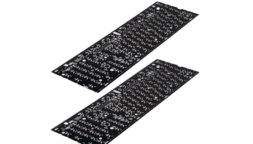
Signal Integrity, EMC, and Power Distribution Benefits
Multi-layer construction enables signal integrity improvements impossible with 2-layer boards, critical for high-performance keyboards.
Controlled Impedance
Reference planes enable precise impedance control. USB 2.0 requires 90Ω differential impedance for reliable high-speed operation. Single-ended signals achieve consistent 50Ω characteristic impedance. Trace geometry combined with known dielectric properties ensures repeatability. Impedance testing validates manufacturing accuracy.
Return Path Quality
Solid reference planes improve signal return paths:
- Reduced Loop Area: Signals return directly beneath traces on adjacent plane.
- Lower EMI: Smaller loop area reduces electromagnetic radiation.
- Improved Noise Immunity: Clean return paths reject external interference.
- Layer Transitions: Via placement must maintain return path continuity.
Power Integrity
Dedicated power planes improve power delivery. Low-impedance distribution maintains voltage under load transients. Decoupling capacitor effectiveness improves with plane connections. Reduced voltage ripple benefits sensitive analog circuits. RGB Backlit Keyboard PCB implementations achieve stable LED operation with proper power planes.
EMC Performance
Multi-layer construction simplifies EMC compliance. Reduced emissions from contained return currents. Improved immunity from external electromagnetic sources. Shield layers provide additional isolation when needed. Pre-compliance testing shows measurable improvement versus 2-layer designs.
Multi-Layer PCB Cost vs Performance Trade-offs
Multi-layer PCBs increase cost, requiring careful consideration of value versus investment.
1. Cost Factors
Understanding cost drivers helps justify multi-layer investment:
- Material Cost: Additional copper and prepreg layers increase raw material.
- Process Complexity: More lamination cycles and drilling operations.
- Yield Impact: Additional layers increase defect opportunities.
- Typical Premium: 4-layer costs approximately 30-50% more than 2-layer.
2. Design for Manufacturing
Multi-layer designs require additional DFM attention. Layer registration affects via alignment tolerance. Aspect ratio limits constrain via diameter versus board thickness. Copper balance prevents warpage during lamination. Stack-up specification must be clearly communicated to manufacturer.
3. Lead Time Implications
Additional layers may affect production schedules:
- Standard Lead Time: 4-layer typically similar to 2-layer at most manufacturers.
- 6+ Layers: May add several days to fabrication schedule.
- Quick-Turn Options: Available but at premium pricing.
- Planning Importance: Account for potential delays in project schedules.
Value Assessment
Multi-layer construction provides value when required performance cannot be achieved otherwise. Wireless performance improvement justifies cost for premium products. Routing capability enables designs impossible with fewer layers. Signal integrity improvements prevent costly redesigns. Mechanical Keyboard PCB Manufacturing services help evaluate cost-benefit for each project.
Whether implementing wireless connectivity, sophisticated RGB lighting, or simply managing complex routing requirements, Multi-Layer PCB for Keyboards provides the capability advanced designs demand. Contact our engineering team to discuss your project requirements and determine the optimal layer count for your keyboard design.
Common Questions
When does a keyboard really need a multi-layer PCB?
Extra layers are justified when wireless design, dense routing, controlled return paths, or complex power distribution cannot be handled cleanly on fewer layers. Many simpler keyboards still work well on standard 2-layer or 4-layer stacks.
What benefits do extra layers provide in keyboard designs?
They improve routing flexibility, power integrity, EMI control, and sometimes wireless performance. The benefit is strongest when the added layers solve a specific electrical or mechanical constraint.
What trade-off should be checked before choosing a higher layer count?
Confirm that the performance gain outweighs the added cost, stackup complexity, and lead time risk. More layers are useful only when they prevent redesigns or enable features the product truly needs.