
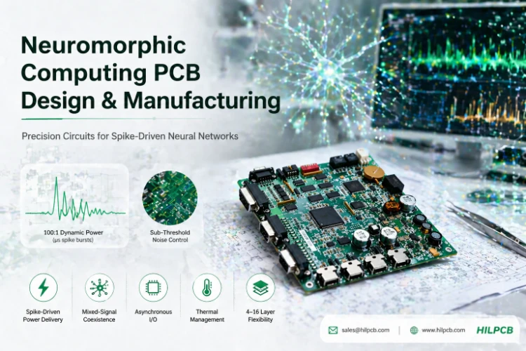
Intel's Loihi 2 processes real-time sensory data at under 1W. IBM's NorthPole achieves 12× the energy efficiency of leading GPUs on image classification. BrainChip's Akida runs on-device learning at milliwatt power. These neuromorphic processors are shipping in production for autonomous robotics, satellite payloads, hearing aids, and industrial inspection — and every one of them presents PCB design challenges that standard digital board practices cannot solve: 100:1 dynamic power swings in microseconds, sub-threshold analog neuron circuits sensitive to microvolt-level noise, and asynchronous event-driven I/O with no clock reference.
HILPCB manufactures neuromorphic computing PCBs from 4-layer research evaluation boards to 16-layer production carrier boards — serving chip developers, research institutions, and product companies deploying brain-inspired computing across automotive, defense, medical, and industrial applications worldwide.
Menu Navigation
- Why Neuromorphic Chips Need Different PCBs
- Power Delivery for Spike-Driven Dynamic Loads
- Mixed-Signal Routing for Sub-Threshold Neuron Circuits
- Event-Driven Sensor and I/O Interface Design
- Thermal Design for Milliwatt-to-Watt Power Swings
- From Research Evaluation Boards to Production Modules
Why Neuromorphic Chips Need Different PCBs
A conventional processor varies perhaps 2× between idle and full load over millisecond timescales. A neuromorphic spiking neural network (SNN) processor varies 100× in microseconds. When quiescent, the chip draws 5 mA. When a burst of spikes propagates through the network — triggered by a visual event from a DVS camera, an acoustic onset from a silicon cochlea, or a tactile contact from a neuromorphic skin sensor — current surges to 500 mA in under 10 μs, then drops back within 50 μs. This is the processor's normal operating mode.
This spike-driven power behavior breaks assumptions embedded in conventional PDN design. Standard decoupling strategies assume smooth current envelopes with superimposed high-frequency noise. Neuromorphic loads are the opposite — the entire power demand is the "transient."
Simultaneously, many neuromorphic architectures use transistors operating in the sub-threshold (weak inversion) regime at 50–300 mV signal levels — 10–100× more noise-sensitive than standard CMOS digital logic. A 1 mV power supply noise spike shifts effective synaptic weight by 5–10%, directly degrading the network's classification accuracy. The PCB must achieve instrumentation-grade noise floors while carrying multi-gigabit host interfaces on the same board.
How Neuromorphic PCB Design Differs
- 100:1 Dynamic Power Range: PDN impedance must maintain regulation across continuous load variation from 5 mA to 500 mA — standard two-point load-step analysis at idle and full power is insufficient for spike-driven loads.
- Sub-Threshold Noise Sensitivity: Board-level noise floors below 100 μV (1 Hz–10 MHz band) required for analog neuron circuits — comparable to precision instrumentation PCBs, not digital processor carriers.
- Broadband Asynchronous EMI: Clock-free handshaking between neuron cores creates spread-spectrum emissions — traditional clock-harmonic filtering is ineffective against this noise pattern.
- Diverse Package Types: Chips from startups and university fabs arrive in everything from standard BGA to custom interposers and chip-on-board — requiring flexible PCB design methodology, not cookbook digital layout.
Power Delivery for Spike-Driven Dynamic Loads
Standard multi-phase VRM designs achieve 100–300 kHz bandwidth (3–10 μs response). Neuromorphic spike bursts arrive in under 10 μs. The decoupling network must absorb entire transient energy while the regulator catches up — thousands of times per second.
PDN Architecture for Neuromorphic Processors
- Ultra-Wideband Decoupling: Three-tier capacitor placement spanning 6 frequency decades — 100 μF polymer for extended spike bursts, 1 μF MLCCs at 2 mm spacing for mid-frequency response, and 10–100 pF within the package shadow for spike-onset transients. Placement optimized through time-domain simulation of actual spiking activity patterns.
- Isolated Analog LDO Power: Separate LDO regulators (>70 dB PSRR at 1 MHz) for sub-threshold neuron power rails — star-point grounding connecting analog and digital ground planes at a single point beneath the neuromorphic IC on multilayer boards (10–16 layers).
- Adaptive Voltage Scaling: VRM with PMBus/I²C voltage programming and <5 μs setpoint response — PDN impedance specification maintained across full 0.5–1.2V dynamic voltage range for spike-activity-dependent power management.
- Real-Time Current Telemetry: High-bandwidth (>1 MHz) current sensing on processor core rail using Kelvin-connected shunt resistors (±0.5% tolerance) — enabling real-time spike activity monitoring and power-aware workload optimization.
Mixed-Signal Routing for Sub-Threshold Neuron Circuits
The core mixed-signal challenge of neuromorphic PCB design is coexistence between sub-millivolt analog sensitivity and multi-gigabit digital signaling on the same board. Analog neuron interface signals at 50–300 mV share board real estate with USB 3.2 (10 Gbps), GbE, PCIe Gen 4 host interfaces, FPGA-based spike sorting logic, and event-driven sensor buses — five distinct signal domains each requiring different impedance, shielding, and isolation treatment.
Mixed-Signal Layout for Neuromorphic Boards
- Physical Domain Separation: Analog neuron circuit power, ground, and signal routing confined to a dedicated board region with continuous ground plane boundaries. Inter-domain connections through a single bridge point with ferrite bead filtering — preventing digital return currents from flowing through analog ground planes.
- Dedicated Ground Plane Architecture: Separate analog and digital ground planes on 10–16 layer constructions, connected at a single star point beneath the neuromorphic IC where the chip's internal analog and digital grounds bond. Via stitching at 2 mm intervals along domain boundaries prevents slot antenna resonance.
- Stripline Signal Isolation: Analog neuron interface traces routed on inner stripline layers with ground shielding above and below — >40 dB isolation from digital signal layers. Minimum 5× trace width spacing between analog and digital signals, or ground-stitched guard traces for tighter constraints.
- Quiet Zone Placement: Sub-threshold bias generators, voltage references, and analog-to-spike converters placed at maximum distance from switching regulators, oscillators, and high-speed connectors — component orientation aligned to minimize capacitive coupling between noisy and sensitive nodes.
Event-Driven Sensor and I/O Interface Design
Neuromorphic processors connect to event-driven sensors generating data fundamentally differently from conventional frame-based devices. A Dynamic Vision Sensor (DVS event camera from Prophesee, iniVation, or Samsung) outputs asynchronous pixel events at microsecond resolution rather than synchronous frames. A silicon cochlea produces spike-encoded audio with 1 μs temporal resolution. A neuromorphic tactile sensor array generates contact events asynchronously across hundreds of taxels.
A 10 μs jitter on event input — insignificant for frame-based systems — corrupts spike-timing-dependent plasticity (STDP) learning algorithms where temporal correlation between events encodes information. The PCB interface must preserve this temporal precision across all sensor channels.
Event Interface PCB Design
- AER Bus Routing: Address-Event Representation bus with ±0.5 ns skew matching across all address and handshake lines — LVDS or sub-LVDS signaling on high-speed PCB layers with 100Ω differential impedance controlling propagation delay variation.
- SPI/QSPI Sensor Link: 50–100 MHz SPI for neuromorphic sensor configuration and event streaming (BrainChip Akida, SynSense Speck/Xylo) — matched trace lengths with ≥3× spacing between clock and data lines.
- Hardware Timestamp Synchronization: PTP-like hardware timestamping (<1 μs accuracy) across all sensor interfaces — common reference clock distribution for multi-sensor fusion combining event camera + IMU + audio on a single neuromorphic carrier board.
- Host Interface Domain Isolation: USB 3.2 or GbE host connections on dedicated signal layers with continuous ground plane separation from neuromorphic processing domain — preventing multi-gigabit switching from contaminating sub-millivolt neural circuits.
Thermal Design for Milliwatt-to-Watt Power Swings
The neuromorphic chip typically dissipates <1W — but the carrier board's supporting electronics (regulators, I/O transceivers, sensor interfaces, communication controllers) collectively produce 5–15W. Many neuromorphic deployment targets — autonomous drones, wearable medical devices, industrial inspection cameras — are fanless, battery-powered, and compact (40×60 mm), requiring all heat extraction through conduction.
Compact Thermal Architecture
- Selective Thermal Via Strategy: Dense thermal via arrays beneath power regulators and I/O transceivers — not under the neuromorphic chip. This reverses conventional thermal patterns that concentrate management under the main processor.
- Copper Thermal Spreading: 2 oz copper inner planes on high-Tg FR-4 spreading regulator heat across the full board area — critical on boards <100×100 mm where concentrated heating creates 30°C localized hot spots.
- Battery-Powered Efficiency: Converter efficiency targeting >90% at typical 200 mW neuromorphic load and >85% at 2W burst — minimizing waste heat in sealed enclosures.
- Industrial Environmental Range: -40°C to +85°C qualification with 1,500+ thermal cycle validation — supporting outdoor robotics, defense, and transportation deployments.
From Research Evaluation Boards to Production Modules
Neuromorphic computing spans an unusually wide maturity range — from university groups fabricating custom chips on shuttle runs (needing 3 boards in 10 days for a grant milestone) to BrainChip and SynSense shipping thousands of production modules. HILPCB supports both ends with identical noise floor and power integrity discipline.
Manufacturing Across Maturity Stages
- Research Evaluation Boards: 2–10 boards for chip bring-up — chip-on-board wire bonding, custom interposers, analog probe access, debug headers. 5–7 day turnaround.
- Development Platforms: 50–200 boards on standardized form factors (COM Express carrier, Jetson-compatible) with production-intent signal integrity for algorithm development.
- Production Modules: 1,000–10,000+ units with automated SMT assembly, ICT, functional test, and conformal coating — SPC-controlled processes maintaining validated noise floor.
- Multi-Chip Module Integration: Neuromorphic processor + event sensor + host interface as single module on HDI PCB with 0.1 mm microvias and analog-grade domain isolation.
Discuss your neuromorphic hardware requirements — from evaluation board to production module →
Frequently Asked Questions
How does a neuromorphic processor's power profile differ from a standard CPU? While a traditional CPU has a relatively smooth power envelope with high-frequency noise, a spiking neural network (SNN) processor sits mostly idle and then surges in power—often by a factor of 100x—in under 10 microseconds when processing a burst of spikes. The PCB's power delivery network (PDN) must be designed to absorb these massive, instantaneous transients without voltage sags.
Why is analog routing so important for neuromorphic chips? Many neuromorphic architectures use sub-threshold analog circuits that operate at 50–300 mV. A noise spike of just 1 mV can alter synaptic weights and degrade the AI's accuracy. This requires the PCB to maintain instrumentation-grade noise floors, heavily shielding the analog neuron signals from multi-gigabit digital interfaces using stripline routing and isolated ground planes.
What is an event-driven sensor interface? Unlike standard cameras that capture frames at 60 FPS, neuromorphic sensors (like DVS event cameras) asynchronously output data only when a pixel changes, offering microsecond temporal resolution. The PCB must route these Address-Event Representation (AER) buses with extreme precision (sub-nanosecond skew matching) to preserve the exact timing of spikes, which is crucial for learning algorithms.
How is heat managed on compact neuromorphic carrier boards? Though the neuromorphic chip itself may draw less than 1 Watt, the supporting electronics (regulators, I/O transceivers, sensors) can generate 5–15W. Because many edge AI applications are fanless and sealed, the PCB acts as the primary heatsink, utilizing heavy inner copper planes and dense thermal via arrays beneath the regulators to spread the heat laterally.