
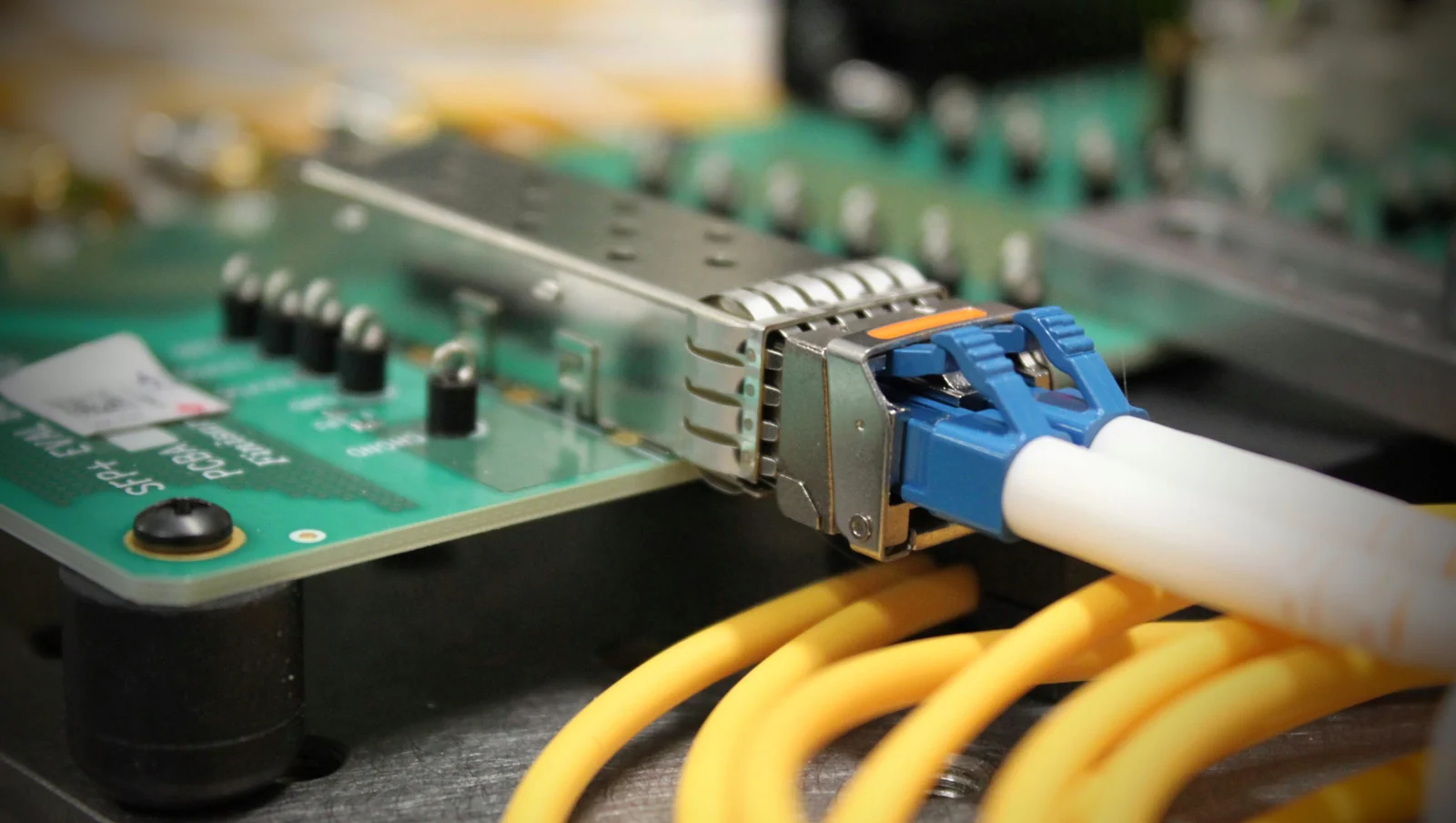
- When an OSFP 800G transceiver PCB is buildable as a sample but unstable in production, the cause is usually not that the middle trace suddenly became worse, but that short and sensitive structures such as connector transitions, local vias, material consistency, thermal paths, and assembly coplanarity consume channel margin first in volume production.
- On this kind of board, what really needs to be frozen is a manufacturable high-speed channel, not only a layout result. OIF's public context around 112G electrical interconnect already makes it clear that local transition zones become visible bottlenecks before long trunks do.
- The thermal problem of an OSFP module board is not an isolated issue. High-power devices, copper distribution, shell contact, and flatness changes all feed back into assembly condition and high-speed consistency.
- Management and monitoring circuits do not dominate main-channel loss, but they directly affect bring-up, compatibility, debug efficiency, and lot traceability.
- A truly reliable OSFP 800G board is not one sample that "runs at 800G," but multiple lots that still behave closely after connector assembly, thermal stress, and manufacturing variation.
Quick Answer
The core of an OSFP 800G transceiver PCB is not just drawing a 112G channel. It is making connector launch, local transitions, thermal path, assembly window, and the validation matrix still hold in production. For high-speed pluggable modules, freezing system boundaries before fine optimization is closer to real delivery conditions.
Table of Contents
- What should engineers review first on an OSFP 800G transceiver PCB?
- Summary table of key rules and parameters
- Why does the connector region always consume channel margin first?
- Why must material choice be judged together with real channel length and thermal path?
- Why do the management interface and assembly window directly affect production stability?
- Why is OSFP 800G validation about consistency instead of one passing result?
- Next steps with HILPCB
- Frequently Asked Questions (FAQ)
- Public references
- Author and review information
What should engineers review first on an OSFP 800G transceiver PCB?
Start with connector transitions, 112G channel budget, thermal path, management interface, and assembly consistency.
This question does not mean "the middle route is short enough, so it is fine," and it does not mean "the module board is smaller than a motherboard, so it should converge more easily." The public OSFP MSA specification already defines the module and connector context, while OIF's public statement on CEI 5.0 concentrates 112G electrical-interconnect risk in higher-frequency and more sensitive transition zones. On a module board, the items that should be frozen first are connector launch, local vias, board-edge precision, thermal contact, and assembly tolerance rather than only the in-board route.
The five questions that are usually most useful early are:
- Whether the connector transmit launch, breakout, and via zone have stable geometry
- Whether the in-board segment is reviewed together with the motherboard side and connector-side budget
- Whether material and stackup match target path length, thermal load, and production variation
- Whether thermal path, shell contact, and flatness will change assembly and electrical behavior in return
- Whether validation covers multiple boards, multiple lots, and post-assembly conditions
If the project is aimed at pluggable high-speed modules, it is usually better to bring the interface rules of High-Speed PCB and Backplane PCB into the review early rather than judging only one internal route on the module board.
Summary table of key rules and parameters
| Rule / Parameter | Recommended range or judgment method | Why it matters | How to verify | What happens if ignored |
|---|---|---|---|---|
| Connector launch | Review breakout, anti-pad, hole copper, and return path together | The connector region usually consumes margin first | Local simulation, TDR, sample observation | The middle route looks fine, but the interface fails first |
| 112G budget | Split motherboard side, connector side, in-board path, and assembly variation first | A module board is not an isolated channel | Channel budget, S-parameters, comparison study | Material and length window are misjudged |
| Material / stackup | Judge Dk / Df together with copper foil, glass style, lamination, and thickness | Nominal low loss does not equal stable production | Datasheet, stackup review, sample comparison | Lot variation gets amplified |
| Thermal path | Review copper distribution, thermal vias, shell contact, and flatness together | Thermal behavior feeds back into SI consistency | Thermal image, hot-state test, assembly observation | Room temperature passes, hot condition becomes unstable |
| Management interface | Keep management, monitoring, and power paths debuggable | Bring-up, compatibility, and traceability depend on them | Bring-up check, management-link validation | Data path works, but the module is not deliverable |
| Assembly window | Review coplanarity, voids, connector posture, and residue together | Assembly directly rewrites final electrical behavior | First-article inspection, X-ray, process record | Sample works, but production spread grows |
| Public module context | Direct implication for design |
|---|---|
| OSFP MSA connector / module definition | Connector and board-edge structures are board-level boundaries from the start |
| OIF 112G electrical interconnect | Budget must be decomposed down to local transitions and assembly variation |
| High-power, high-speed module | Thermal path and flatness feed back into SI and assembly consistency |
Why does the connector region always consume channel margin first?
Conclusion: Because the largest number of discontinuities are stacked in the smallest space.
The connector zone of an OSFP module board combines pads, anti-pads, via transitions, reference-plane changes, and local return-path limits at the same time. OIF's public context around 112G electrical interconnect already shows that the first place to lose control on a high-speed module board is often not the mid-route trunk, but this kind of short and dense local structure.
The first questions worth confirming are:
- Whether the connector launch and breakout zone keep stable geometry
- Whether anti-pad, capture pad, and return vias fit the current speed grade
- Whether local hole-copper consistency and surface finish amplify lot variation
- Whether the transition zone has already been tied to real factory tolerance instead of only nominal models
Many cases where "the route is not long, but the channel still fails" are really cases where the connector region has already consumed the margin first. On pluggable high-speed modules, it is usually better to confirm the local transition window of High-Speed PCB at the front end rather than watching only the trunk segment.
Why must material choice be judged together with real channel length and thermal path?
Conclusion: Because the loss budget and stability of an OSFP 800G module board are never determined by one in-board segment alone.
The on-board path of a module has to be judged together with the motherboard side, module connector side, package side, and assembly state. If the team only compares Dk / Df values in datasheets without checking path decomposition and thermal path, material selection easily turns into over-specification. On this kind of module board, a more reasonable review usually includes:
- Putting motherboard launch, module connector, board route, and device interface into one budget
- Checking whether the current path length actually reaches the point where a lower-loss material is necessary
- Checking whether copper roughness, glass style, lamination stability, and thickness variation will amplify differences
- Checking whether thermal design will feed back into material and structural behavior
The best material choice is therefore usually not the most expensive material, but the one that keeps loss, thermal behavior, and production variation inside the same controllable window. If the module board also combines high layer count with fine-pitch mixed assembly, it is also worth bringing the stackup control of Multilayer PCB into the judgment of materials and thermal path.
Why do the management interface and assembly window directly affect production stability?
Conclusion: Because deliverability of an OSFP module depends not only on the data path, but also on whether the module remains initializable, diagnosable, and repeatable after assembly.
Management and monitoring circuits do not dominate main-channel loss, but they directly affect initialization, compatibility, field diagnosis, and lot traceability efficiency. If those low-speed networks are pushed casually into crowded high-speed zones, or if the assembly window is not frozen early, many later problems become hard to reproduce.
More useful early actions usually include:
- Keeping management and monitoring loops away from the most aggressive high-speed transition zones
- Placing temperature, current, or state sensors closer to the true thermal condition
- Freezing connector coplanarity, voids, connector posture, and residue control
- Planning serial information and production traceability logic during the design phase
For projects approaching pilot build, it is better to plan these assembly inputs together with SMT Assembly and PCB Prototype instead of adding the traceability logic only after samples return.
Why is OSFP 800G validation about consistency instead of one passing result?
Conclusion: Because the only valuable release condition is that connector transitions, material, thermal path, and assembly window have all been proven under the same validation logic.
For an OSFP 800G module board, the validation loop should be built around whether high-speed, electrical, thermal, and assembly data can explain one another, rather than around one eye diagram or one BER result. A truly reliable process window does not prove only that one sample "runs at 800G." It proves that the structure can be built repeatedly.
A practical pre-release checklist usually includes:
- Connector and transition freeze. Are launch, breakout, anti-pad, and key via structures already frozen?
- Material and stackup freeze. Have low-loss material, copper foil, and dielectric-control assumptions been reviewed together?
- Thermal-path freeze. Are hotspot distribution, heat-spreading strategy, and shell-contact approach clear?
- Assembly-window freeze. Are stencil, reflow, void control, and connector posture already written into the process plan?
- Validation-matrix freeze. Are insertion loss, return loss, temperature rise, management response, and lot traceability all defined clearly?
If the project is already close to pilot production, it is usually better to organize these inputs directly into Quote / RFQ or front-loaded engineering notes instead of judging design maturity from one sample alone.
Next steps with HILPCB
If you are currently moving forward with an 800G optical module, an OSFP interface board, or another dense high-speed module, the next step is usually to turn "it can be sampled" into "it is a manufacturable high-speed channel."
- When the main issue is connector launch and 112G budget, first use the High-Speed PCB path to converge the local transition structure.
- When the module must also work with a system-side high-speed board or backplane, use Backplane PCB to review the interface boundary together.
- When thermal path, copper distribution, and local hotspots have become key constraints, check the heat-spreading path of High-Thermal PCB at the same time.
- When assembly and sample validation need to move forward together, pushing key checkpoints into SMT Assembly and PCB Prototype exposes issues earlier.
- When connector transitions, material, thermal path, and validation matrix are all clear, organizing them into Quote / RFQ makes it easier to explain the full boundary in one pass.
Frequently Asked Questions (FAQ)
Which section should be checked first on an OSFP 800G module board?
A: Usually the connector transmit launch and breakout zone, not the long middle route. The local geometry and return path there consume channel margin first.
Does an OSFP 800G board always need the highest-grade material?
A: Not necessarily. The need for a higher-grade material depends on real path length, the number of connector transitions, thermal path, and production-consistency requirements, not on the material label alone.
Why can a thermal problem become a high-speed consistency problem?
A: Because in high-power modules, the thermal path affects flatness, assembly condition, and material behavior, and those changes eventually return to electrical behavior.
Can assembly variation really affect the high-speed result directly?
A: Yes. Coplanarity, voids, connector posture, residue, and reflow history can all change final channel behavior or long-term reliability.
What is most worth freezing before fabrication?
A: Freeze connector transitions, material and stackup, thermal path, assembly window, and the validation matrix first. The later those are frozen, the more rework cost appears in pilot build.
Public references
OSFP MSA Specification
Supports the article's explanation of the public module and connector-specification context for OSFP.OIF Releases Common Electrical I/O CEI 5.0 Implementation Agreement
Supports the article's explanation of the public context around OIF 112G electrical interconnect.OIF Implementation Agreements Index
Adds background that the public context around 112G-generation electrical interconnect and management continues to evolve.
Author and review information
- Author: HILPCB Optical Interconnect Content Team
- Technical review: SI, thermal-design, and assembly engineering team
- Last updated: 2026-05-20