
Featured
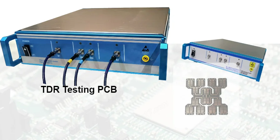
TDR Testing PCB: Advanced Quality Control for Mission-Critical Electronics
Define PCB TDR testing with impedance targets, coupons, rise time, fixtures and reports. Compare production acceptance with channel diagnostics and VNA measurements.
Expert insights on PCB manufacturing, assembly excellence, and cutting-edge electronic technologies
Your trusted partner for professional PCB manufacturing and assembly solutions
Define PCB TDR testing with impedance targets, coupons, rise time, fixtures and reports. Compare production acceptance with channel diagnostics and VNA measurements.
Understand UFS embedded storage, MIPI M-PHY signal integrity, power rails, routing and assembly verification for compact electronic devices.
Deep dive into Boundary-Scan/JTAG (IEEE 1149.1), covering test, debug, and ISP for high-density optical module PCBs, with SI, thermal management, and power/interconnect considerations to support NPI EVT/DVT/PVT.
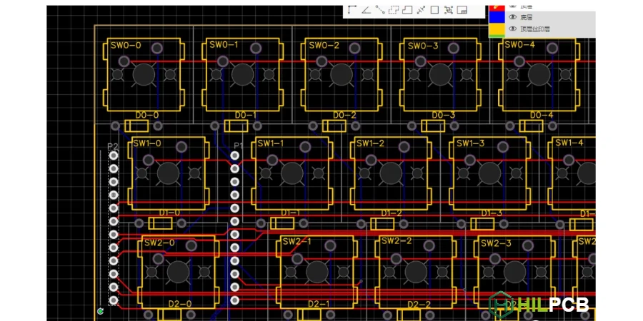
Generate correct Gerber and drill files for keyboard PCB production. Covers layer mapping, plated and non-plated holes, KiCad export, release checks and fabrication or assembly handoff.
Plan LED screen PCBs around pixel geometry, driver timing, power drop, thermal paths and module testing. Compare practical fabrication and assembly options.
Plan level-sensor PCBs around the sensing method, tank installation, antenna, duty-cycle power and network architecture. Includes a battery calculation and manufacturing RFQ.
Plan portable medical imaging PCB fabrication and assembly around isolation drawings, thermal and battery budgets, material compatibility, risk controls and ordered test records.
Data-center demand response needs a verified EMS-to-BMC control chain, metering and safe power transitions. Select PCB construction and assembly tests from the actual server or gateway design.
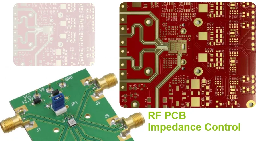
Control RF PCB impedance from stack-up through fabrication and TDR/VNA verification, with coupon, tolerance, failure-analysis and RFQ decision tables.
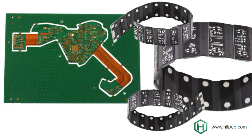
Plan rigid-flex fabrication around region-by-region stackups, bend use, vias, coverlay, impedance and mechanical tolerances. Review HILPCB manufacturing routes and prepare a build package.
Design turbidity sensor PCBs around the optical method, low-leakage analog chain, calibration, power and data quality. Prepare fabrication, assembly and integration requirements for water-monitoring instruments.
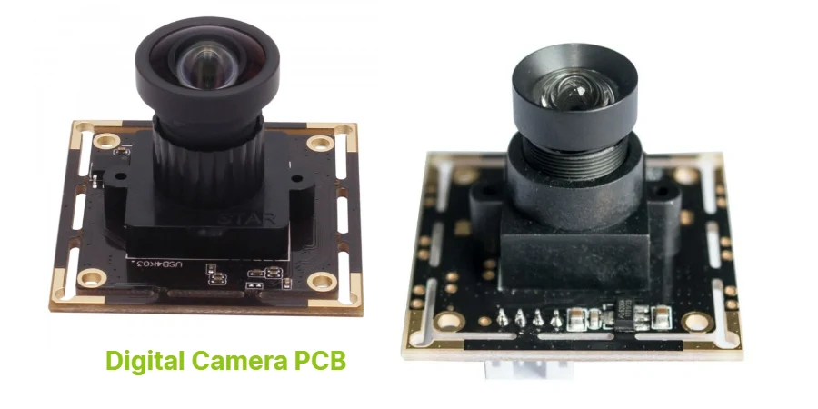
Choose a digital camera PCB around sensor bandwidth, power noise, thermal paths and optical alignment. Define fabrication, assembly and image-test scope before sourcing.