
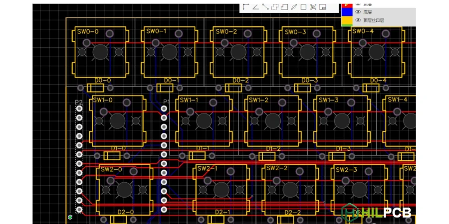
The final step in keyboard PCB design is generating manufacturing files that accurately communicate your design to the fabrication facility. Gerber files—the industry-standard format—describe each PCB layer as drawing commands. Errors in file generation can result in incorrect boards, manufacturing delays, or rejected orders.
HILPCB accepts Gerber files from all major PCB design software and provides design review to catch potential issues before production.
In This Guide
- Understanding Gerber File Layers
- Drill File Formats and Generation
- Supported PCB Design Software
- KiCad Export Process (Example)
- Gerber Verification Before Submission
- Assembly Files: BOM and Position Data
- File Organization and Manufacturer Specifications
Understanding Gerber File Layers
Gerber files use RS-274X format (Extended Gerber), the industry standard for decades. Each file describes one layer as a series of drawing commands that manufacturing equipment interprets to produce physical features.
Required Files for 2-Layer Keyboard PCB
| File | Extension | Description |
|---|---|---|
| Top Copper | .GTL | Traces, pads, copper pours on top |
| Bottom Copper | .GBL | Traces, pads, copper pours on bottom |
| Top Solder Mask | .GTS | Mask openings for soldering |
| Bottom Solder Mask | .GBS | Mask openings on bottom |
| Top Silkscreen | .GTO | Component labels, graphics |
| Bottom Silkscreen | .GBO | Labels on bottom (if used) |
| Board Outline | .GKO/.GM1 | PCB edge, must be closed path |
Optional Files
- Paste Layers (.GTP, .GBP): Solder paste stencil openings—required for assembly orders
- Drill Drawing: Visual hole representation—helpful but not required
Copper layers define conductive features. Solder mask layers define mask openings (negative logic). Silkscreen prints on top of mask. Board outline must be a single continuous closed path.
Drill File Formats and Generation
Excellon is the standard drill file format—ASCII text containing tool definitions and hole coordinates.
Typical Keyboard Drill Sizes
- Vias: 0.3-0.4mm
- Switch pins: 1.27mm
- PCB-mount pins: 1.7mm
- Stabilizer housing: 3.0mm
- Mounting holes: 2.2mm (M2)
PTH vs NPTH
Plated Through-Holes (PTH): Copper-plated for electrical connection—switch pins, vias, component leads.
Non-Plated (NPTH): Mechanical only—mounting holes, alignment pins, stabilizer screws.
Best practice: Generate separate PTH and NPTH files. Use millimeters with decimal format for clarity.
Essential Gerber Files
Supported PCB Design Software
HILPCB accepts Gerber files from all standard PCB design software. The Gerber format (RS-274X) is universal—properly generated files work regardless of which tool created them.
Popular PCB Design Tools
Professional/Commercial:
- Altium Designer: Industry-standard professional tool with comprehensive Gerber export
- Cadence OrCAD/Allegro: Enterprise-level PCB design suite
- Mentor PADS/Xpedition: Professional PCB design with advanced features
- Zuken CR-8000: High-end design for complex boards
Accessible/Hobbyist-Friendly:
- KiCad: Free, open-source, extremely popular in keyboard community
- EasyEDA: Free web-based tool with integrated ordering
- Autodesk Eagle: Long-established tool, free version available (KiCad vs Eagle compared)
- Autodesk Fusion 360 Electronics: Integrated mechanical/electronics design
- CircuitMaker: Free community-based tool from Altium
Specialized:
- Diptrace: Affordable professional-grade tool
- Target 3001!: German software with strong European following
- DesignSpark PCB: Free tool from RS Components
Common Export Features
All these tools export standard RS-274X Gerber and Excellon drill files. Specific menu locations and options vary, but the output format is identical. The following section uses KiCad as a detailed example—similar concepts apply to other software.
KiCad Export Process (Example)
KiCad is popular in the keyboard community due to its open-source nature and excellent keyboard-specific libraries. This walkthrough demonstrates the export process—similar steps apply in other EDA tools.
Gerber Export (File → Plot)
Output directory: Create dedicated folder (e.g.,
./gerber/)Format: Select "Gerber"
Layers to plot:
- F.Cu, B.Cu (copper)
- F.SilkS, B.SilkS (silkscreen)
- F.Mask, B.Mask (solder mask)
- Edge.Cuts (board outline)
- F.Paste, B.Paste (if ordering assembly)
Options:
- Enable "Plot reference designators"
- Enable "Check zone fills before plotting"
- Enable "Use Protel filename extensions" (for universal .GTL, .GBL naming)
- Coordinate format: 4.6 (millimeters)
Drill File Export
- Click "Generate Drill Files" from Plot dialog
- Format: Excellon
- Units: Millimeters
- Zeros format: Decimal
- PTH/NPTH: Merge or separate per manufacturer preference
- Click "Generate Drill File"
Final Steps
Click "Plot" to generate all Gerber files. Verify output directory contains all expected files before proceeding to verification.
Gerber Verification Before Submission
Never submit manufacturing files without verification. A few minutes of checking prevents incorrect boards.
Free Gerber Viewers
- Gerbv: Open-source, Linux/Windows
- KiCad Gerber Viewer: Familiar interface for KiCad users
- ZofzPCB: 3D visualization reveals issues not obvious in 2D
- Tracespace.io: Web-based, no installation required
- Reference Gerber Viewer: Many manufacturers provide online viewers
Verification Checklist
File completeness:
- All expected layers present and non-empty
- Drill file(s) included
Board outline:
- Single closed path
- Correct overall dimensions
Copper layers:
- All traces complete without gaps
- Copper pours filled correctly
- No unintended features
Solder mask:
- Openings align with copper pads
- Appropriate clearance around pads
Silkscreen:
- Text readable
- Doesn't overlap pad openings
Drill alignment:
- Overlay copper + drill to verify holes center on pads
- All expected holes present
Assembly Files: BOM and Position Data
When ordering assembled boards, additional files guide component procurement and placement.
Bill of Materials (BOM)
Essential fields:
- Reference designator (matches silkscreen)
- Value
- Footprint/package
- Manufacturer part number (critical for correct procurement)
- Quantity
Export from your EDA tool—most provide BOM generation. CSV format is universally accepted.
Position/Centroid Files
Provide X/Y coordinates and rotation for automated pick-and-place:
- Reference designator
- X position, Y position
- Rotation angle
- Board side (top/bottom)
Critical: Verify position file origin matches Gerber origin. Mismatched origins cause systematic placement offset.
Standard Keyboard PCB Specifications
File Organization and Manufacturer Specifications
Recommended Folder Structure
keyboard-v1.0/
├── gerber/
│   ├── keyboard-F_Cu.GTL
│   ├── keyboard-B_Cu.GBL
│   ├── keyboard-F_Mask.GTS
│   ├── ... (all Gerber files)
│   └── keyboard.DRL
├── assembly/
│   ├── BOM.csv
│   └── positions.csv
└── README.txt
README Contents
Document essential specifications:
- Project name, version, date
- Layer count, dimensions, thickness
- Copper weight, surface finish
- Solder mask color, silkscreen color
- Any special requirements
Package as: keyboard-v1.0-gerbers.zip
Standard Keyboard Specifications
Most keyboards use these cost-effective parameters:
- Layers: 2
- Thickness: 1.6mm
- Copper: 1oz (2oz for RGB-heavy)
- Finish: HASL (economical) or ENIG (flat pads, hot-swap friendly)
- Mask: Various colors available
HILPCB Capabilities
HILPCB accepts all standard Gerber formats:
- RS-274X: Universal standard
- Gerber X2: Enhanced with embedded metadata
- Excellon: Drill files
- ODB++: Available on request
Manufacturing capabilities:
- 2-64 layers
- Standard 3/3mil (75μm) at standard pricing
- Advanced 2/2mil (50μm) when required
- 24-48 hour quick-turn for standard builds
HILPCB Manufacturing Services
HILPCB simplifies the manufacturing process:
Design Review: We validate Gerber format, layer alignment, and DFM issues—feedback within 24 hours for standard designs.
Fabrication: Standard PCB with multiple surface finish and mask color options.
Assembly: Prototype assembly for development, turnkey production for volume.
Submit your keyboard Gerber files—our team verifies integrity and provides feedback before production begins.