
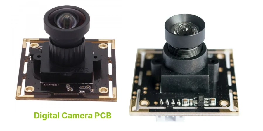
A digital camera PCB may be a small sensor carrier, a processor and storage mainboard, or a board that also drives the lens and wireless link. Define that boundary first: it determines the interconnects, power rails, cooling, mechanical datums and tests that the manufacturer must support.
HILPCB provides multilayer and HDI fabrication, SMT assembly and turnkey component sourcing for these builds. The manufacturing review connects the released sensor and processor choices to stackup, BGA escape, assembly access and production tests. Lens alignment, image calibration and finished-camera qualification need their own defined equipment, procedures and ownership; they are separate from making and electrically testing the board.
Digital Camera PCB Architecture and High-Speed Image Processing
A camera architecture selects the functions needed for its imaging mode and output interface. Common blocks include:
- CMOS or CCD image sensors with the output and readout electronics specified by the selected device; CSI-2 and LVDS are examples, not interchangeable electrical interfaces
- An application processor, MCU, FPGA or dedicated imaging device sized for the processing workload
- An Image Signal Processor (ISP), integrated or separate, for the required color, noise and image-processing pipeline
- GigE Vision, USB3 Vision or CoaXPress connectivity when required by the machine-vision host
- Memory and storage interfaces sized for buffering, compression and recording
- A suitable Wi-Fi, Bluetooth or cellular module when wireless transfer is part of the product
- Lens actuators and their matching drivers where autofocus, zoom or stabilization is needed
- Exposure, position or other measurement circuits not already integrated into the sensor or processor
Choose the layer count after BGA escape, reference planes, rail distribution and the mechanical outline are known. A multilayer PCB may resolve the routing without HDI; use high-speed PCB stackup and transition review where the actual channel budget requires it. An 8–12-layer architecture is one possible design choice, not a camera-industry minimum.
For a first bandwidth estimate, active image payload = width × height × frames per second × bits per pixel. An explicitly assumed 3840 × 2160, 60 fps, 12-bit raw stream carries about 5.97 Gb/s of active image data. Dividing across four D-PHY data lanes gives about 1.49 Gb/s per lane before transport overhead. Use the sensor's actual line timing, packetization, blanking behavior and available lane rates to establish the required margin; multi-exposure HDR or additional streams can change the budget.
MIPI CSI-2 is an imaging protocol that can use different physical layers, including D-PHY and C-PHY. Layout and connector rules must follow the selected transmitter, receiver and PHY. HDI PCB technology is useful when the sensor or processor escape and board area justify microvias; it does not by itself establish shock resistance or image quality.
Advanced Manufacturing for Digital Imaging Devices
Translate the application into manufacturing decisions rather than assigning one construction to every camera type:
- Sensor carriers: finish, flatness, fiducials and mounting datums compatible with the sensor package and optical assembly
- Action cameras: routing density, flex or board connectors, component support and access for mechanical attachment
- Surveillance cameras: power input, protection, thermal path and selected coating or enclosure integration
- Machine vision: trigger and synchronization interfaces, connector transitions and test access
- Processor mainboards: reference planes, memory escape, stackup and placement/reflow risks
- Wireless cameras: antenna keep-outs, shield access and a coexistence test plan for the assembled product
HILPCB's SMT assembly route includes SPI, AOI and selected X-ray, with fine-pitch and hidden-joint requirements reviewed against the actual build. Turnkey assembly assigns BOM sourcing, alternates and supplied-part ownership, while programming and functional testing follow the agreed firmware, fixture and limits. State separately whether the order also needs sensor cleanliness controls, optical alignment or image calibration; these cannot be inferred from a general electrical-test scope.
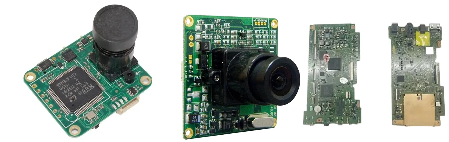
Power Management and Signal Integrity Optimization
Power and thermal budgets must cover the camera's operating modes, not just its average idle current:
- Sensor and processor rails: follow the device sequencing, ripple, load-step and decoupling requirements; distinguish analog-rail noise from the processor's current demand
- Battery cameras: budget recording, standby, wireless transmission and actuator peaks separately, including converter efficiency and usable battery capacity
- Surveillance cameras: size PoE input or another supply for the selected sensor, processor, infrared lighting, heater and startup behavior
- Machine vision: define supply transients, grounding, cable interfaces and continuous-duty load at the installation
- Power-state changes: verify capture, storage and wireless activity together so rail droop or noise does not corrupt the intended operating mode
- Heat removal: establish the processor/sensor-to-enclosure path and acceptable temperatures in continuous recording
- Construction choice: consider high thermal PCB options for a justified heat path, while preserving the signal layers and sensor mounting geometry required by the design
Keep switch-node, motor and radio-current loops away from sensitive sensor rails and analog paths. Plan continuous return paths for high-speed channels and verify the package reference design before adding ground splits or filters. An electrical rail measurement and a captured image under the same operating load reveal different problems; include both when noise artifacts are an acceptance risk.
Digital Camera PCB Applications and Market Segments
Digital Camera PCB technology serves diverse imaging and vision market segments:
- DSLR PCB for Professional Photography and Studio Equipment
- Action Camera PCB for Sports, Adventure, and Content Creation
- Surveillance Camera PCB for Security Systems and Smart City Infrastructure
- Machine Vision PCB for Industrial Automation and Quality Control
- Photography PCB for Mirrorless Cameras and Hybrid Video Systems
- Camera Circuit Board for Smartphone and Mobile Device Integration
- Automotive Camera PCB for ADAS, Backup Cameras, and Dash Cam Systems
- Medical Imaging PCB for Endoscopy, Dental, and Diagnostic Equipment
- Broadcast and Video Capture where sustained recording, output bandwidth and cooling define the board workload
- Scientific Imaging, including microscopy and astronomy, where exposure modes, sensor temperature and calibration requirements shape the acceptance plan
Machine-vision inspection, surveillance analytics and photography can share fabrication methods while needing different acceptance tests. A triggered industrial camera may prioritize timing and dropped-frame checks; a low-light camera may prioritize image noise at specified exposure and gain. The camera PCB overview covers the broader integration decisions.
Comprehensive Ecosystem Solutions for Camera Development
The following functions belong in the design and sourcing package when they are part of the product. Their presence in a camera architecture does not make them standard deliverables in every PCB order:
Image Sensor Integration:
- The selected CMOS or CCD device/module, its exact variant and handling requirements
- Sensor trigger, exposure and synchronization connections for machine vision
- Mechanical and electrical interfaces for compact sensor carriers
- Per-sensor timing, data aggregation and calibration ownership for multi-camera arrays
Optical System Components:
- Lens actuator type, driver requirements and position feedback for autofocus or zoom
- Gyroscope/accelerometer orientation and actuator-control interfaces for stabilization
- LED flash or xenon strobe circuits when required, including their power and safety constraints
- Infrared-cut mechanisms and optical switching for day/night use; selected image-intensifier architectures add a different high-voltage supply scope, discussed in night vision PCB integration
Connectivity and Storage:
- SD or CFexpress interfaces with the required sustained recording rate and host support
- USB-C or another product connector with its specified data, power and mechanical functions
- Wireless modules selected for throughput, power, antenna placement and approvals
- Firmware and network-service ownership for streaming or cloud storage, separate from bare-board fabrication
Supporting Hardware and Mechanical Integration
Board outline, sensor location and assembly datums should be released with the mechanical design. For example, a sensor-carrier datum error can affect optical alignment even when every net passes electrical test; specify the datum and measurement method rather than relying only on a general board-outline tolerance.
Environmental Solutions:
- Define the finished enclosure's ingress-protection target, seals, connectors and test conditions; a bare PCBA has no automatic IP67/IP68 rating
- Select component temperature, lifecycle and qualification requirements for the actual program rather than a generic “military-grade” label
- Set mounting, connector retention and assembled-product shock/vibration requirements for the expected use
- Define operating/storage temperatures and image-calibration behavior across the intended temperature range
User Interface Integration:
- Touch-screen LCD controllers for DSLR PCB menu systems and image review
- Electronic viewfinder interfaces for mirrorless Camera Circuit Board designs
- Voice control integration for hands-free Action Camera PCB operation
- Remote control receivers for professional Photography PCB applications
Lens and Motor Control:
- Precision stepper motor drivers for DSLR PCB autofocus and zoom systems
- Ultrasonic motor controllers for silent video Photography PCB operation
- Aperture control systems for professional Camera Circuit Board applications
- Image stabilization actuators for handheld and Action Camera PCB use
Why Choose HILPCB for Digital Camera PCB Manufacturing
HILPCB's multilayer, high-speed and HDI routes support different camera layouts. Standard multilayer routing is appropriate when it meets escape and channel requirements; HDI adds microvia and via-in-pad options for denser layouts. Its high-speed service includes controlled-impedance stackup and TDR/VNA correlation, selected to the actual channel and coupon plan rather than applied as a blanket imaging specification.
The SMT service lists ISO 9001 quality-system controls and IPC-A-610/J-STD-001 workmanship by order; an IPC acceptance class is not a camera-product certification. Prototype and NPI review can connect the released revision to stencil/profile settings, inspection results and customer-defined electrical or functional tests. Where the product needs enclosure, cable and firmware integration, box build assembly adds that scope under a defined system-test plan.
Send the board files, stackup intent, BOM/approved alternates, placement file, quantity and sourcing responsibilities. For a sensor carrier, add sensor datums, connector/flex drawings and handling restrictions; for a processor board, add the image modes, channel/lane rates and thermal limits. Include any firmware, test charts, illumination conditions, fixture interfaces and pass/fail limits required for image testing. This lets the quote separate board fabrication, component supply, assembly/tooling and optical or system-test work, so competing offers cover the same deliverable.
Camera programs can draw on HILPCB's SI and thermal engineering, image-sensor calibration and optical-integration support, and sourcing or integration of sensor, lens, strobe and storage modules. Environmental and ruggedness tests can be arranged to the product's operating profile, with the test provider and equipment identified in the project scope. These services support camera development without implying a universal layer count, HDI requirement, or product certification.
Frequently Asked Questions About Digital Camera PCB Manufacturing
Does every high-resolution camera need HDI or 8–12 layers?
No. Resolve sensor/processor escape, reference planes, memory routing, power and the outline first. Use a conventional multilayer construction when it meets those constraints; use HDI where microvias or finer escape justify the additional process cost.
How should camera image-data bandwidth be estimated?
Multiply active width, height, frame rate and transmitted bits per pixel for a payload starting point. Then use the actual sensor mode, transport timing, extra streams and PHY limits to select lane count and rate. The assumed 3840 × 2160, 60 fps, 12-bit example above is about 5.97 Gb/s before overhead.
What helps a camera survive outdoor or action-camera use?
Review the board mounting, connectors, thermal path, coating compatibility and enclosure seals against the specified environment. Coating, rigid-flex or an industrial component label alone does not establish finished-product shock or ingress performance; test the released assembly and enclosure to the program's conditions.
Does PCB assembly include optical alignment and sensor calibration?
These must be separately defined. Electrical testing can verify rails, interfaces and programmed behavior; optical alignment and image calibration also require the correct mechanical datums, lens/sensor arrangement, controlled target and illumination, software and image limits. Agree the process owner and quoted coverage before release.
Can HILPCB support consumer and machine-vision camera boards?
Its fabrication, SMT and turnkey routes can be reviewed for sensor carriers, processor boards and camera-control assemblies. Supply the interface and package details, mechanical requirements, quantity and acceptance plan so the actual build can be assessed. Product-specific image quality, cybersecurity, medical or automotive qualification remains a defined system-level activity.