
PCB hole-to-hole spacing is often checked as the laminate web between production drill edges, not the space between pad edges or finished openings. There is no universal minimum: get the selected fabricator's rule for the hole types, materials and process, then check electrical reliability separately. One published fabrication rule uses 0.25 mm (10 mil) between drill-tool edges; it is a useful comparison point, not an IPC requirement or a promise for every board.
For finished-hole sizing and pin fit, use the finished hole size and drill tolerance guide. This article focuses on the remaining material between neighboring holes, the actual geometry of via fields, and what to agree before release.
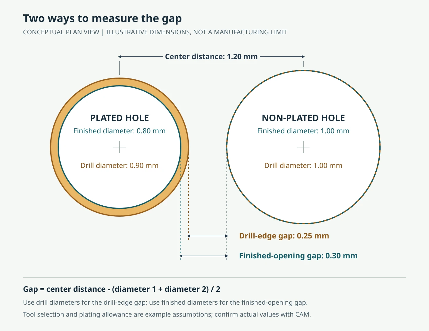
Conceptual illustration; the dimensions are an example, not a manufacturing limit.
View the full-size illustration
1. Identify the Two Edges Before Applying a Number
| Measurement | Reference | Use |
|---|---|---|
| Center-to-center | Hole center to hole center | Coordinate-based input to the calculation |
| Finished-hole gap | Edges of finished openings | Assembly and CAD checks where finished diameters are specified |
| Drill-tool gap | Edges of the selected production tools | Nominal material web for a fabricator's drill-edge rule |
| Copper-to-copper gap | Edges of pads, barrels or other copper features | Separate electrical clearance check on each relevant layer |
For two round holes, using a common unit throughout:
Here C is center distance and D1 and D2 are the production tool diameters, not necessarily the diameters in the design file. The same equation using finished diameters gives the finished-opening gap. For equal drills it simplifies to Wtool = C-D.
For plated holes, the production drill is generally larger than the specified finished opening. The actual allowance depends on the fabricator and process. One published fabricator example uses a 0.10 mm increase in diameter for PTH and no increase for NPTH; do not assume either allowance applies to a different order. State whether the drill file contains finished sizes and let CAM confirm its tool choices. Do not pre-compensate production data and then let the fabricator compensate it again.
Worked example: unequal plated and non-plated holes
Suppose a plated hole has a 0.80 mm finished diameter, a nearby NPTH has a 1.00 mm finished diameter, and their centers are 1.20 mm apart. For this illustration only, CAM proposes a 0.90 mm PTH drill and a 1.00 mm NPTH drill:
The nominal finished-opening gap is 1.20-(0.80+1.00)/2=0.30 mm. Applying the full 0.10 mm PTH allowance to both holes would incorrectly give 0.20 mm. Against a hypothetical 0.25 mm tool-edge requirement this layout is exactly on the nominal threshold, with no extra design margin. Request a CAM review rather than treating the calculation as approval; selected tool sizes, center registration, drill tolerances and the supplier's definition of its minimum still matter. Avoid subtracting a tolerance twice if it is already included in the supplier's rule.
Translate a tool-edge rule into a finished-hole DRC
If the CAD rule measures finished-opening edges, and CAM has confirmed the tool diameter for each hole, define a1 and a2 as the respective diameter increases from finished opening to tool. The equivalent nominal check is:
For the mixed-hole example, 0.25+(0.10+0.00)/2=0.30 mm. A finished-opening DRC set to 0.25 mm would therefore miss a nominal 0.05 mm of required web for this pair. This conversion is not a tolerance stack or a safety margin; use the supplier's agreed rule basis, and confirm how the CAD tool actually measures the pair. Different hole classes or tool selections may require different rules.
2. Separate the Decisions
| Hole pair or concern | First decision | What must still be checked |
|---|---|---|
| Two PTHs on different nets | Compare tool-edge web with the supplier's rule for that construction | Barrel/pad copper spacing, voltage, environment and CAF qualification |
| Two PTHs on the same net | Confirm the permitted mechanical web and drill sequence | Nearby copper, other nets and assembly requirements; same-net status is not a waiver for the rest of the layout |
| PTH next to NPTH | Confirm each actual tool and the mixed-hole rule | NPTH-to-copper clearance, fastener and mechanical loads |
| Overlapping holes or a slot | Flag the geometry for CAM review | Define an intended slot as a slot, including plating and tolerances; agree the manufacturing route |
| Laser microvia or blind/buried via | Identify layer span, drill process and neighboring conductive features | Depth overlap, sequential-lamination rules and process-specific reliability |
Published supplier limits differ. A second fabricator lists 0.45 mm for different-net component PTHs and 0.30 mm for vias at standard 1 oz copper, but its short help page does not define the edge reference. Another article lists 6 mil via-to-via and 0.30 mm PTH-to-PTH edge spacing without resolving the tool-versus-finished basis. These figures cannot be compared directly until the reference and process are confirmed; none establishes HILPCB's minimum.
The web is not an electrical clearance measurement. Check pad-to-pad and hole-to-copper rules on every applicable layer, including inner layers and antipads. For safety insulation, apply the product's applicable standard and construction requirements separately. Surface creepage, air clearance and internal solid insulation are different checks; a drill-edge DFM pass is not proof of any of them.
3. Calculate the Actual BGA Via Field
Ball pitch alone is not necessarily via pitch. A uniform, equally offset fan-out preserves the ball grid spacing, but alternating offsets, staggered escape patterns and nearby component holes can make another pair closer. Use exported via coordinates and the fabricator's tool diameters to check pairs with overlapping drill spans. For non-overlapping spans, ask CAM about drill sequence and construction-specific rules rather than assuming they are exempt. Also check copper and layer-specific spacing independently.
The following are geometry examples, assuming equal-size through-vias on a square grid with identical offsets. They are neither recommended hole sizes nor a fabrication or reliability approval:
| Via-grid pitch | Assumed tool diameter | Orthogonal tool-edge web | Diagonal tool-edge web |
|---|---|---|---|
| 1.00 mm | 0.30 mm | 0.70 mm | 1.11 mm |
| 0.80 mm | 0.30 mm | 0.50 mm | 0.83 mm |
| 0.65 mm | 0.25 mm | 0.40 mm | 0.67 mm |
| 0.50 mm | 0.20 mm | 0.30 mm | 0.51 mm |
For this specific square grid, the center distances are p orthogonally and √2p diagonally, so subtract the tool diameter in each case. A staggered layout needs its own coordinate-based distances. For example, adjacent 0.80 mm-pitch ball centers with via offsets of +0.10 mm and -0.10 mm toward each other have via centers only 0.60 mm apart; two 0.30 mm tools leave 0.30 mm, not the 0.50 mm shown for uniform offsets.
If a check fails, consider moving vias, revising the escape, or discussing a smaller drill and its aspect ratio with the fabricator. A blind microvia or via-in-pad changes the construction and qualification problem; it is not an automatic CAF or cost fix. The annular ring guide covers the separate copper-ring trade-off around these holes.
4. CAF Is a Qualification Question, Not a Pitch Formula
Conductive anodic filamentation (CAF) is an internal insulation failure mechanism associated with conductive paths in the laminate between biased conductors. Moisture, voltage, laminate construction and fabrication conditions can affect risk. Hole-to-hole geometry is one concern; hole-to-plane and other conductor pairs may also need review. A same-net pair normally has little or no differential bias in service, but it does not eliminate risks involving other nearby nets.
A drill-spacing minimum establishes the supplier's manufacturing boundary for its stated conditions. It does not establish product life, a safe voltage, or CAF resistance. Do not use a generic fourth-power relationship to convert BGA pitch into service life: a model fitted to one experiment cannot establish failure times for a different material, drill process, voltage and environment.
High glass-transition temperature (Tg) is a thermal property, not a CAF qualification result. A laminate marketed as CAF resistant is also not a substitute for an agreed test on a representative construction. When comparing material data, ask for the exact grade and construction, specimen geometry, conditioning, voltage, temperature, humidity, duration, failure criterion and number of samples. A test pass under one set of conditions does not establish field lifetime under another.
What to ask the qualification owner
- Which conductor pairs carry the largest sustained or intermittent differential bias, and what is the smallest relevant web?
- What service humidity, temperature, contamination exposure, life and safety requirements apply?
- Does the proposed coupon represent the material grade, glass styles, stackup, hole sizes, separation, conductor geometry and manufacturing route of the board?
- What test method and revision, preconditioning, bias, temperature, humidity, duration, sample size and failure threshold will be agreed? Specify the required report and disposition of failures.
- Who approves substitutions or a change in drilling, laminate or layer construction, and when must qualification be repeated?
CAF testing and surface insulation resistance testing address different failure geometries. Agree the test method and coupon with the qualification owner rather than assuming a generic SIR result proves hole-to-hole CAF performance. Microsections and bare-board electrical tests can support a manufacturing investigation but do not by themselves establish long-term CAF life.
5. DRC and Fabrication Release
Designer: Export the real hole locations, sizes, plating status and layer spans; identify different-net neighbors and critical voltage domains. Ask whether the design-rule checker uses finished openings, drill tools or another edge. For a finished-hole-based check, calculate an appropriate rule from the confirmed allowance for each hole pair; use separate constraints or a CAM check if one offset cannot represent the mixed sizes and hole types. Preserve finished-hole requirements in the delivered files unless CAM agrees otherwise.
Fabricator: Confirm the tool-size basis, minimum web for the actual material and drilling route, tolerances already included in that limit, and the planned response to narrow webs or overlapping drills. Review annular ring, hole-to-copper, slots and any proposed geometry changes. A smaller tool also needs a finished-size and plating feasibility check.
Quality and procurement: Include the approved stackup and laminate grade, relevant voltage and operating environment, fabrication drawing revision, and the specific coupon and evidence requested. Agree the test scope, sample quantity, acceptance criteria and handling of substitutions in the quotation and purchase documents. Do not infer that a routine bare-board test includes CAF qualification.
HILPCB lists standard, mid-Tg and high-Tg FR-4 PCB review, with CAF-resistant or customer-specified grades as options. Availability and test scope depend on the order. Send the layout, hole table, stackup and operating requirements with a quote request and agree the applicable drill-spacing and qualification requirements before release.
Frequently Asked Questions
What is the minimum PCB hole-to-hole spacing?
There is no single minimum for all boards. One published fabrication rule uses 0.25 mm between drill-tool edges, while other published supplier values differ and may use an unclear reference. Confirm the rule for the selected fabricator, material, hole types and process.
Is the gap measured from finished holes or drill tools?
It depends on the rule. A drill-edge rule uses the selected production tool diameters; a CAD check may use finished openings. State the reference explicitly and have the fabricator confirm any plated-hole compensation.
Can same-net holes be closer than different-net holes?
Some suppliers allow different mechanical and electrical rules, but do not assume a universal same-net minimum. Confirm the fabrication rule and check nearby conductors, copper spacing and mechanical requirements.
Does passing the drill-spacing rule prevent CAF?
No. Manufacturing spacing is not a CAF life rating. Review the actual material, geometry, bias and environment, and agree representative coupon testing and acceptance criteria where the application requires it.
Is BGA ball pitch the same as via-to-via spacing?
Only for particular layouts, such as a uniform grid with identical via offsets. Staggered offsets or nearby holes can create a smaller separation; calculate from actual via centers and tool sizes.