
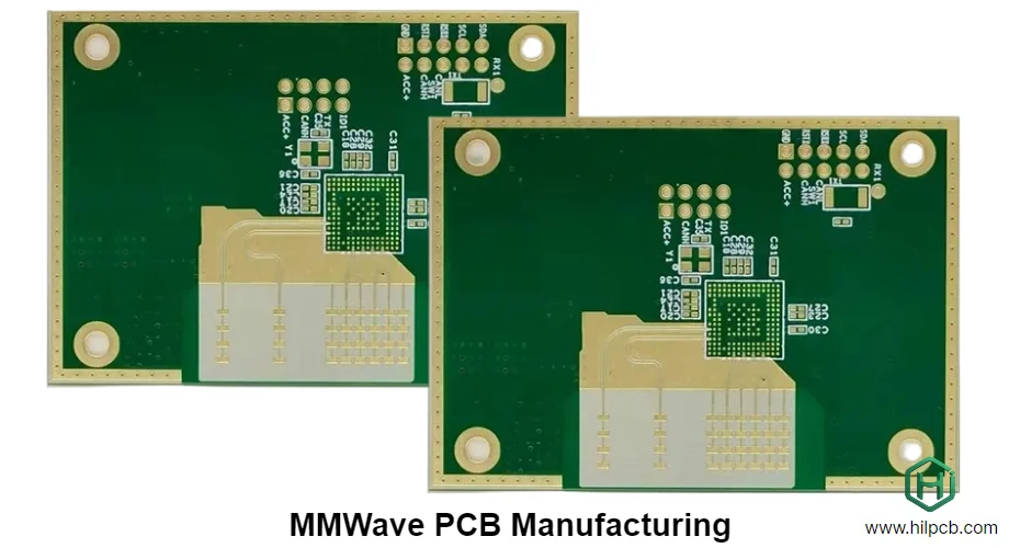
In 5G/6G communication systems—especially applications built on Massive MIMO and Beamforming—phase accuracy is the lifeline that determines system performance. To deliver high-performance RF front-end modules on tight schedules, Phase consistency routing quick turn has become a core yardstick for PCB design and manufacturing capability. It not only demands extremely tight delay matching on physical routing, but also represents a systems engineering challenge spanning materials science, electromagnetic theory, and precision fabrication. From an RF front-end engineer’s perspective, this article explores the key techniques and challenges behind achieving excellent phase consistency.
Core challenge: why phase consistency is foundational in 5G/6G RF design
5G/6G systems use antenna arrays to focus energy in specific directions via beamforming, improving antenna gain and spectral efficiency. The physical basis is the Huygens principle: by precisely controlling the feed-network phase for each antenna element, signals add constructively in the target direction and cancel in others.
Any phase error in the feed network directly causes beam pointing deviation (Beam Squint), gain loss, increased sidelobe level (Sidelobe Level), and can even destabilize the entire link. In FR2 (24.25–52.6 GHz) mmWave bands, the very short wavelength means even micron-level physical length differences can become meaningful phase offsets. That is why strict Phase consistency routing is a prerequisite for meeting 3GPP requirements and achieving high throughput and reliable connectivity.
Transmission-line selection: trade-offs among microstrip, stripline, and CPWG
Choosing the right transmission-line structure is the first step toward phase-consistent routing. Different structures trade off performance, manufacturing cost, and integration flexibility.
- Microstrip: A simple structure consisting of a signal trace, dielectric substrate, and a bottom ground plane. It is easy to fabricate, place components on, and debug. However, part of the field is exposed to air, making it more susceptible to external interference, with higher radiation loss and stronger dispersion (different phase velocity across frequency), which complicates phase control at mmWave.
- Stripline: The signal trace is embedded between two ground planes in a homogeneous dielectric. This symmetric structure provides excellent shielding, very low radiation loss, and much lower dispersion than microstrip—ideal for long, high-precision clock or LO distribution. The downside is difficulty in probing inner-layer routing and tighter manufacturing tolerances on dielectric thickness and uniformity.
- Grounded Coplanar Waveguide (GCPWG): The signal trace and adjacent ground copper are on the same layer with a reference plane underneath. GCPWG combines microstrip’s debug convenience with stripline-like shielding, and integrates well with on-board mmWave devices. By adjusting the signal-to-ground gap, impedance and field distribution can be tuned flexibly, making it a common FR2 choice.
Transmission-line structure comparison
| Feature | Microstrip | Stripline | GCPWG |
|---|---|---|---|
| Signal isolation | Poor | Excellent | Good |
| Radiation loss | High | Very low | Lower |
| Dispersion | Significant | Minor | Controllable |
| Manufacturing/debug convenience | High | Low | Medium |
| Recommended use | Sub-6 GHz, short-distance matching | High-precision clock/LO distribution | mmWave (FR2), chip interconnect |
Phase consistency routing materials: low-loss substrates and copper-foil roughness
Materials are the physical foundation of RF performance. Selecting the right Phase consistency routing materials is critical for controlling loss and phase consistency. Key parameters include:
- Dielectric constant (Dk): Dk stability and consistency directly affect characteristic impedance and phase velocity. Local Dk variation causes phase mismatch, so select high-performance materials with minimal Dk drift versus frequency and temperature.
- Dissipation factor (Df): Df reflects how strongly the dielectric absorbs electromagnetic energy and is a major contributor to dielectric loss. At mmWave frequencies, low-Df materials (e.g., PTFE/Teflon) are essential to reduce total insertion loss.
- Copper-foil roughness: At mmWave, Skin Effect concentrates current near the conductor surface. Rough copper increases the effective current path length, raising conductor loss and phase-velocity dispersion. Low-roughness or Reverse Treated copper helps reduce high-frequency loss.
Materials such as Rogers PCB and other PTFE-based high-frequency PCB options are preferred for mmWave thanks to strong Dk/Df performance and tight thickness tolerances. To achieve Phase consistency routing cost optimization, a Hybrid Stack-up that uses expensive RF materials only on critical RF layers while using standard FR-4 on non-critical layers (power and digital control) is a common, proven approach.
mmWave placement and routing: key techniques for vias, shielding, and isolation
Meticulous placement and routing are what turn design intent into real performance. In mmWave PCB design, every detail can become a bottleneck.
- Via fence: One or more rows of dense ground vias placed along both sides of microstrip or CPWG routing can suppress parallel-plate modes, improve isolation, and provide a well-defined return path. Via pitch is commonly recommended to be smaller than 1/8 to 1/20 of the wavelength at the operating frequency.
- Transition via optimization: Layer-change signal vias create impedance discontinuities that can cause reflections and mode conversion. Mitigation includes using the smallest feasible vias, surrounding the signal via with ground vias to maintain return-path continuity, and using Backdrilling to remove unused via stub to reduce resonance in high-speed designs.
- Corner treatment: Avoid 90-degree corners on high-speed traces because they introduce impedance discontinuities and extra radiation. Use multi-segment 45-degree bends or smooth arcs to maintain phase continuity.
- Shielding and isolation: Sensitive circuits such as PLL, VCO, and LNA require strict isolation measures: physical partitioning, keep-out zones, and metal shielding cans when necessary to prevent noise coupling. These measures underpin compliance with Phase consistency routing compliance requirements.
📡 mmWave RF layout: high-frequency EM design sign-off checklist
Signal-integrity and beam-consistency control for 24 GHz–77 GHz+ bands
Physical rule: mmWave signals are extremely sensitive to the return path. Minimize magnetic-flux loop area by keeping reference planes tightly coupled. Do not route across splits; keep return-path impedance flat across the band.
Physical rule: Conventional vias behave like low-pass elements at mmWave. Implement Via Tuning, cage the signal via with a ground-via array, and compensate L/C parasitics in simulation.
Physical rule: For multi-channel MIMO or LO distribution networks, enforce absolute phase symmetry. Use H-Tree structures to balance electrical length and keep inter-channel phase error within a very small range.
Physical rule: Go beyond rules of thumb. Use CST/HFSS for 3D full-wave simulation to capture corner reflections and edge parasitic radiation. All critical RF paths must be validated with both S-parameters and Smith charts.
In mmWave bands, laminate dielectric roughness can dominate loss. We recommend ultra-low-loss PTFE materials plus pulse-plating processes to keep trace edges steep and help your project reach extreme detection precision.
PA/LNA matching networks and bias design: balancing efficiency and stability
Power amplifiers (PA) and low-noise amplifiers (LNA) sit at the core of the RF front end. Matching network design directly affects gain, efficiency, and noise figure.
- Matching networks: The goal is conjugate matching between source and load across the operating bandwidth. Account for package parasitics (bond-wire inductance, lead capacitance) and design with Smith charts. In layout, place matching components (typically high-Q inductors and capacitors) as close to device pins as possible to reduce parasitics.
- Bias networks: Bias networks provide the PA/LNA DC operating point while blocking RF energy from leaking into the supply. Common methods include high-impedance quarter-wave lines or series RF Choke, plus multiple bypass capacitors (from pF to uF) for broadband decoupling to suppress supply noise and parasitic oscillation.
Filtering and clock distribution: keeping signals clean and synchronized
Signal purity in RF systems depends on high-quality filtering and clock/LO distribution networks.
- Filters: Depending on the application, choose SAW, BAW, or discrete LC filters. SAW/BAW filters offer small size and high Q and are often used in Sub-6 GHz. At mmWave, process limitations typically favor distributed filters based on microstrip or waveguide structures. Focus on insertion loss and out-of-band rejection during design.
- Clock/LO distribution: In MIMO and phased-array systems, a highly stable reference clock or LO must be distributed precisely to multiple channels. The network must maintain very low Phase Noise, Spur, and phase offset between outputs. Tree or daisy-chain topologies are common, with precise length matching on each segment to achieve strict Phase consistency routing.
📡 HILPCB manufacturing capability: precision processes that protect phase consistency
Advanced LDI and vacuum lamination provide physical-layer reliability backing for 5G/6G mmWave links
With compensation algorithms and real-time vision scanning, we keep trace-width tolerance within ±10% or better. By reducing etch undercut (Undercut), we maintain consistency of impedance and group delay for high-speed signals.
High-precision vacuum presses and specialized resin-flow control keep dielectric thickness extremely uniform. This stabilizes Dk across the panel and helps prevent beam offset in multi-channel antenna arrays.
Replacing traditional exposure with LDI direct write enables micron-level feature resolution. Inner-layer registration error is minimized, supporting strict anti-pad alignment and stub control in mmWave circuits.
We execute TDR differential/common-mode impedance testing on 100% of builds. Each shipment includes quantified test reports to close the loop between design intent and manufacturing output, ensuring high return-loss performance for RF front-end modules.
From design to manufacturing: process control for automotive-grade Phase consistency routing
Even with a perfect design, manufacturing variation can break phase consistency. For high-reliability applications such as V2X, achieving automotive-grade Phase consistency routing requires tighter control of fabrication tolerances.
Key manufacturing control points include:
- Etching accuracy: Small trace-width changes directly impact characteristic impedance and phase velocity.
- Lamination precision: Non-uniform dielectric thickness causes Dk variation.
- Registration accuracy: Misalignment between layers affects via behavior and stripline symmetry.
Choosing a partner like HILPCB with advanced processes and strict quality systems is critical. They can provide end-to-end support—from material selection recommendations and DFM reviews to precision fabrication and final testing—so design targets are faithfully reproduced in hardware. With prototype assembly, you can validate designs quickly and shorten development cycles.
Phase consistency routing cost optimization: strategies to balance performance and budget
High-performance materials and precision processes protect phase consistency, but cost control is also essential for commercialization. Phase consistency routing cost optimization is not simply cutting cost; it is achieving the best value through smart design and process choices.
- Hybrid stack-up: As noted earlier, using expensive RF laminates only on RF layers while using standard FR-4 on digital/power layers in a multilayer PCB is a mature, widely used cost-reduction strategy.
- Relax non-critical tolerances: Work with your manufacturer to define what is truly critical (e.g., mmWave feedlines) versus non-critical so you avoid unnecessarily tight requirements across the entire board.
- Optimize panel utilization: Consider standard panel sizes during panelization to improve utilization and reduce material waste.
- Select appropriate material grades: Within performance constraints, choose lower-cost Phase consistency routing materials. For example, in Sub-6 GHz, moderate-loss materials may be sufficient without resorting to top-tier mmWave laminates.
Common Questions
Why is phase consistency foundational in 5G/6G RF design?
Because phased-array and MIMO performance depends on precise relative phase between channels. If routing and materials introduce channel-to-channel phase error, beam direction, gain, and overall link stability all degrade.
How should teams choose among microstrip, stripline, and CPWG?
The choice depends on loss, shielding, manufacturability, and tuning needs. Microstrip is easier to access and tune, stripline gives stronger shielding and more stable impedance, and CPWG is often useful when tight grounding and connector transitions matter.
Why do low-loss laminates and copper roughness affect phase consistency?
Both dielectric loss and conductor roughness change attenuation and phase delay, especially at mmWave frequencies. Stable low-loss materials and smoother copper make channel behavior more predictable and easier to match.
How do manufacturing tolerances affect phase consistency and cost?
Etching, lamination, and registration variation directly change impedance and phase velocity. Teams usually protect the truly critical RF paths with tighter controls and premium materials, then relax non-critical areas to balance performance and budget.
Conclusion
Phase consistency routing quick turn is a system-level challenge spanning 5G/6G RF PCB design, simulation, material selection, and manufacturing. It requires not only mastery of electromagnetic theory, but also a deep understanding of material behavior and process boundaries. From selecting the right transmission-line structure and low-loss Phase consistency routing materials, to optimizing every detail of mmWave layout—and ultimately working closely with a reliable manufacturing partner—only then can you turn a design blueprint into a high-performance product that meets strict Phase consistency routing compliance requirements. While pursuing peak performance, applying Phase consistency routing cost optimization smartly is key to winning in the market. With deep RF and mmWave experience, HILPCB is committed to providing one-stop solutions from prototype to volume production and helping you seize the 5G/6G wave.