
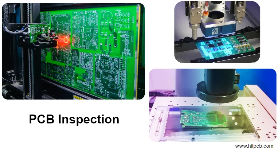
1. Executive summary: data-driven quality commitments and business KPIs
In today’s high-frequency, high-speed, high-density electronics market, PCB is no longer a simple carrier for components—it’s a core determinant of product performance, reliability, and lifecycle stability. At HILPCB, we believe manufacturing excellence is not accidental. It is built on precise quantification, continuous monitoring, and systematic improvement across every process step. The central theme of this whitepaper—process capability analysis pcb—is the foundation that enables this commitment.
Our quality goals are tied directly to measurable business outcomes:
- First Pass Yield (FPY): our target is bare board FPY consistently above 99.5%, and PCBA FPY above 99.2%—translating to lower customer TCO and more predictable deliveries.
- CPK (Process Capability Index): for critical characteristics (trace/space, drilling accuracy, impedance control), we hold to CPK ≥ 1.67. This indicates very low variation (6-Sigma level) and reduces quality risk at the source.
- On-Time Delivery (OTD): enabled by stable capability and disciplined operations, our standard multilayer OTD is 98%+, accelerating customer Time-to-Market.
This whitepaper explains how HILPCB turns these metrics into customer advantage through quantified manufacturing capability, rigorous quality tools, comprehensive test strategy, and end-to-end traceability. We cover the practical use of SPC and MSA, show our SMT and test practices, and include a DFM/DFT/DFR checklist to help build a transparent and efficient co-design / co-manufacturing ecosystem.
2. Core manufacturing capability: quantified precision and stability
At its core, process capability analysis compares design specifications (customer requirements) to real manufacturing variation (our capability). A credible PCB manufacturing whitepaper must be backed by data. HILPCB performs long-term capability evaluation and data collection across all major processes—so we can not only “do it,” but do it consistently at scale.
HILPCB key process capability metrics (mass production)
The table below shows selected capability parameters, control metrics, and production examples—direct evidence of HILPCB’s high-reliability promise.
| Process step | Key capability | Performance metric | Mass production case |
|---|---|---|---|
| Innerlayer imaging | Min. trace/space | 2.5/2.5 mil (63.5/63.5 µm) | CPK > 1.67 |
| Drilling | Min. mechanical drill | 0.15 mm (6 mil) | Hole position accuracy: ±25 µm |
| Plating | Max. aspect ratio | 18:1 | Copper uniformity: >90% |
| Impedance control | Impedance tolerance | ±5% (typ.), ±3% (limit) | TDR pass rate > 99.9% |
| Solder mask | Min. solder mask dam | 3 mil (76.2 µm) | Registration accuracy: ±35 µm |
| Surface finish | ENIG | Au: 1–3 µ" / Ni: 120–240 µ" | Salt spray > 48 hours |
| Lamination | Max. layer count | 40 layers | Layer-to-layer registration: ±50 µm |
Behind these numbers is disciplined gerber data preparation and precise tuning of production equipment. From the customer’s Fab Drawing to the final physical product, we reproduce details reliably. For example, in solder mask fabrication, we combine advanced LDI (laser direct imaging) with best practices aligned to our soldermask exposure tutorial, ensuring solder mask dam integrity and accuracy—building a solid foundation for downstream SMT.
3. Quality-management toolbox: a closed loop from prevention to improvement
Strong manufacturing capability requires a scientific quality system to maintain and improve it. At HILPCB, quality is not limited to Final Inspection—it is process control embedded at every step. We apply proven quality tools to build a closed loop from prevention and monitoring to continuous improvement:
SPC (Statistical Process Control): we use control charts (e.g., X-bar & R) to monitor key parameters (etch rate, plating current density, lamination temperature) 24/7. Any trend approaching control limits triggers alerts, enabling intervention before defects are created.
CPK (Process Capability Index): CPK is our core metric for process stability. We routinely analyze 100+ critical characteristics and keep CPK above 1.67—quantifying our consistency and reliability promise and serving as the measurable outcome of process capability analysis pcb.
Capability highlight: what CPK > 1.67 means When a process CPK exceeds 1.67, the mean is close to the spec center and the distribution width (6σ) is far smaller than the tolerance window. In theory, the defect rate drops below 3.4 DPMO—meeting the widely recognized Six Sigma quality level.
MSA (Measurement System Analysis): data is only as credible as the measurement system. We run Gage R&R studies to ensure AOI, X-Ray, TDR, and other inspection equipment stay within acceptable measurement error so decisions are based on reliable data.
8D (Eight Disciplines): when a quality issue occurs, we launch a structured 8D process—from team formation and problem definition, to containment, root cause, permanent corrective actions, and system-wide prevention—so issues are eliminated and do not recur.
Digital dashboard: SPC data, equipment OEE, line FPY, and other KPIs feed into a centralized dashboard. Management and engineers see quality status in real time and make transparent, data-driven decisions.
4. SMT/assembly process capability and defect control
PCB value is ultimately realized at the assembled functional level. HILPCB’s PCBA services follow the same capability-analysis discipline to connect bare board quality to functional performance.
Our SMT lines use top-tier placement platforms (e.g., Fuji NXT III) with theoretical placement accuracy up to ±25 μm @ 3σ, supporting 01005 components and 0.35 mm pitch BGA.
Key SMT process control points
- Solder paste printing: 3D SPI provides 100% inspection for paste volume/area/height/offset—preventing paste-driven defects (insufficient solder, bridging, misalignment) at the source.
- Component placement: flying cameras and high-resolution component libraries protect placement accuracy and reduce defects like misplacement and tombstoning.
- Reflow soldering: we define a dedicated reflow profile per product and validate with multi-channel profilers to ensure consistent solder joint quality.
- Post-reflow inspection: 3D AOI plus X-Ray for hidden joints (BGA, QFN) to detect cold joints, voids, and Head-in-Pillow.
With tight control across these steps, we maintain a continuous yield improvement roadmap that reduces defect rates over time.
5. Full-stack test coverage: ensuring reliability in real environments
Quality is not only manufactured—it is also verified. HILPCB provides full-stack testing from component level to system level. Our test coverage philosophy is “layered defense, each layer with a focus” to maximize defect detection and ensure stable field performance.
| Test method | Description | Coverage scope | Defects detected | Applicable products |
|---|---|---|---|---|
| AOI | Image-based inspection for soldering and component appearance. | 100% SMT joints, polarity, wrong/missing parts. | Bridging, solder balls, tombstoning, offset, wrong part, reverse. | All SMT assemblies |
| ICT | Probe-based test points to measure component parameters. | R/C/L values, diode/transistor characteristics, opens/shorts. | Wrong values, component failure, cold joints, opens/shorts. | Mid/high-density, high-value boards |
| FCT | Simulate end-use and verify full PCBA function. | I/O signals, interfaces, power management, logic. | Design issues, software bugs, parameter drift. | All products requiring functional validation |
| Hipot Test | Apply high voltage to verify insulation and clearance. | Insulation of power and high-voltage circuits. | Breakdown, insufficient clearance, leakage current out of spec. | Power, industrial control, medical |
| Reliability test | Stress testing for long-term stability. | Temp cycling, vibration, shock, salt spray. | Early-life failures, material fatigue, insufficient design margin. | Automotive, aerospace, outdoor |
We follow a standardized hipot test procedure to ensure safety and accuracy. By combining these methods, we tailor test plans to the product and optimize cost vs. quality.
6. End-to-end traceability: a data chain from materials to field
When issues occur, the ability to localize root cause quickly and isolate affected lots is critical. HILPCB’s traceability system builds a complete data chain from raw materials to shipped products—and, when applicable, field usage.
- Unique identity: every PCB panel and unit receives a unique QR code or serial number.
- Process data binding: the unique ID is bound to key data across the flow, including:
- Material info: laminate lot, component Reel ID.
- Equipment and parameters: machine ID and settings at each step (placement force, reflow profile, etc.).
- Personnel: operator and inspector IDs.
- Test data: detailed ICT/FCT logs and results.
- Data lake and visualization: all data is consolidated into a manufacturing data lake. With visualization tools, we can trace any PCB’s complete history in seconds. For example, if a field failure correlates to a specific BGA lot, we can identify all products using that lot and analyze whether production data shows common anomalies.
This traceability system is not just for problem solving—it is a continuous-improvement data engine that powers process capability analysis pcb with large-scale real production data.
7. DFM/DFT/DFR checklist: best practices for collaborative design
The most successful projects come from tight design-manufacturing collaboration. To help customers reduce manufacturing, test, and reliability risk at the design source, we provide this DFM/DFT/DFR checklist. Following it improves yield, shortens development cycles, and reduces total cost.
HILPCB collaborative checklist (V2.0)
This checklist summarizes years of experience—from fab drawing essentials to advanced reliability considerations.
| Category | Check item | Best practice / recommendation |
|---|---|---|
| DFM (Manufacturing) | Gerber Data Preparation | Provide RS-274X or ODB++ with clear layer definitions. |
| Trace/space | Avoid absolute limits; keep at least 10% design margin. | |
| Pad design | Use NSMD for BGA pads; recommended pad size is 80–85% of ball diameter. | |
| Via type | Prefer through vias; use blind/buried vias cautiously. For VIPPO, specify fill and capping requirements clearly. | |
| Solder mask bridge | Ensure sufficient solder mask dam for dense pins (e.g., QFP), recommended ≥ 3.5 mil. | |
| Silkscreen | Do not print on pads; character height ≥ 30 mil; line width ≥ 5 mil for readability. | |
| Panelization | Use V-cut or mouse-bites; provide clear panel drawing; keep edge clearance (≥ 5 mm). | |
| Plane-to-pad clearance | Keep ≥ 8 mil between planes and non-connected pads/holes to avoid shorts. | |
| Fiducial marks | Place 2–3 fiducials on panel/unit diagonals; 1 mm diameter, 2 mm soldermask opening. | |
| Annular ring | Ensure adequate annular ring for all PTH (≥ 4 mil) to prevent opens. | |
| ... (15+ more items) | ... | |
| DFT (Test) | Test points | Provide ≥ 0.8 mm diameter test points for critical signals; spacing ≥ 1.5 mm. |
| Test-point distribution | Distribute points evenly; avoid crowding in one area. | |
| ICT accessibility | Do not place points under large components or within 3 mm of the board edge. | |
| JTAG/Boundary Scan | Break out TCK, TMS, TDI, TDO, TRST for JTAG-enabled ICs. | |
| Programming interface | Reserve ISP/SWD or similar for firmware programming and debug. | |
| Power isolation | Add 0Ω resistors or jumpers to isolate power domains for test. | |
| ... (5+ more items) | ... | |
| DFR (Reliability) | Component selection | Avoid EOL or single-source components. |
| Thermal management | Add thermal vias under high-power devices and increase ground copper area. | |
| Decoupling capacitors | Place close to IC power pins per datasheet recommendations. | |
| ESD protection | Add ESD devices near external ports (USB, HDMI, etc.). | |
| Material selection | Select laminates based on frequency, temperature, and environment (e.g., FR-4 TG170, Rogers). | |
| ... (5+ more items) | ... |
8. Win-win collaboration: a HILPCB case study and your next step
Case study: yield improvement for a medical diagnostics customer
A leading medical-device manufacturer developing a next-generation portable ultrasound probe faced PCBA yield below 90%, mainly due to intermittent BGA solder failures.
HILPCB intervention and solution
- Joint analysis: our engineers performed X-Ray and cross-section analysis and found the root cause: improper VIPPO process control created micro-voids inside BGA joints.
- DFM optimization: based on process capability analysis pcb data, we recommended VIPPO design optimizations and updated gerber data preparation rules for soldermask openings.
- Process improvement: we developed a dedicated vacuum reflow profile and implemented 100% 3D X-Ray inspection—forming a customized yield improvement roadmap.
- Results: after three iterations, PCBA FPY improved to 99.6% and field failure rate dropped by 85%. The customer not only solved the quality issue but also pulled in the launch schedule by two months.
This case reflects HILPCB’s value: we are not only a manufacturer—we are a professional partner on your product realization path. Excellent quality starts with transparent communication and deep technical collaboration.
Start your high-reliability project now
Ready for data-driven manufacturing services? HILPCB invites you to work with our expert team to turn your design into reliable, scalable products.
Upload your Gerber and BOM to receive a free DFM/DFT analysis report within 24 hours.
Let’s define the next standard for high-quality electronics through precision capability analysis and seamless collaboration.
FAQ
What does process capability analysis actually tell a PCB or PCBA team?
It shows whether a manufacturing process can repeatedly stay inside the required specification limits instead of only passing occasional samples. In practice, capability analysis helps teams judge if drilling, printing, placement, reflow, or other key steps are stable enough for reliable scale-up rather than relying on isolated inspection results.
Why is a good yield number alone not enough to prove process capability?
Because a single yield result only shows what happened in one batch, while capability analysis measures whether the process remains centered and controlled over time. A line can deliver a decent short-term yield and still be drifting toward future defects if variation, setup discipline, or material behavior are not truly under control.
Which process steps most often deserve capability analysis in electronics manufacturing?
The highest-value targets are the steps that directly affect fit, solder quality, electrical reliability, or repeatability, such as solder paste printing, pick-and-place accuracy, reflow stability, drilling, plating, impedance control, and critical inspection data. Teams get the most value when they focus on processes that influence both yield and downstream reliability.
How should capability analysis connect with DFM, DFT, and continuous improvement?
It should be used as a feedback loop, not a separate quality report. The data should inform design tolerances, fixture strategy, test coverage, process-window decisions, and corrective actions so teams improve the product and the production line together instead of reacting only after defects appear.
Conclusion
This article explains process capability analysis pcb in practice—CPK, yield improvement, quality tools, test coverage, and traceability—and provides a DFM/DFT/DFR checklist to help teams control risk across design, materials, and test. By following the checklist and operating within proven process windows—and by involving HILPCB’s DFM/DFA team early—you can accelerate prototypes and mass production without sacrificing quality and compliance.
For manufacturing and assembly support, contact HILPCB via Turnkey Assembly or SMT Assembly to get DFM/DFT recommendations.