
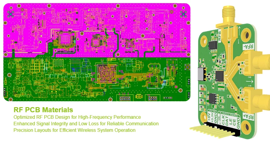
As 5G evolves into the mmWave band and 6G technologies are explored, RF Front-End requirements have reached unprecedented levels. In this context, RF front-end low noise PCB manufacturing is no longer “just making a board”; it is an engineering discipline combining materials science, EM theory, precision manufacturing, and microwave measurement. As a microwave measurement engineer, I know that tiny deviations from design to final product can catastrophically degrade system performance. Especially for highly integrated RF front-end modules that demand low NF and high linearity, the PCB itself is a key part of system performance. From a measurement perspective, this article breaks down de-embedding, fixtures and probes, S-parameter consistency, OTA testing, and failure localization—practical guidance for 5G/6G challenges.
De-embedding methods: TRL, LRM, SOLT boundaries and errors
At microwave frequencies, any connector, transmission line, or fixture introduces its own electrical behavior and “pollutes” the true evaluation of the DUT. The core goal of De-embedding is to mathematically remove these parasitics via precise Calibration and extract the DUT’s clean S-parameter results.
Calibration method comparison
SOLT (Short-Open-Load-Thru): the most traditional method, relying on precisely defined standards. It is mature for coax environments. On planar PCB structures, however, it’s extremely difficult to manufacture ideal broadband open (fringing capacitance) and load (no parasitic L/C) standards—especially in mmWave—so accuracy is limited.
TRL (Thru-Reflect-Line): the gold standard for planar measurements. It does not require an ideal load; instead it uses a Thru, a high Reflect (often open/short), and a Line with known length. These standards are much more consistent on PCB than SOLT, so TRL can achieve excellent accuracy. Its main drawback is that bandwidth depends on the Line length (typically 1/4 wavelength), so multiple Lines are needed for wideband coverage.
LRM (Line-Reflect-Match): a TRL variant that can be advantageous in some cases. It uses line and reflect standards as well, but replaces the Thru with a Match load. The load does not need to be an ideal 50Ω, but it must be identical at both ports—often easier with symmetric fixture designs.
In the RF front-end low noise PCB prototype stage, TRL is critical for accurate device modeling. In RF front-end low noise PCB mass production, test flows may be simplified, but Test Limit settings must be derived from precise measurements obtained earlier (such as TRL).
Probe stations and fixtures: transition effects and repeatability control
Fixtures and probes are the physical bridge between the VNA and the PCB DUT; their quality directly defines the ceiling of your measurement results. A poor fixture can make an excellent chip or PCB look mediocre.
Transition effects and optimization
The transition region from coax to planar PCB transmission lines (microstrip or CPW) is a key SI bottleneck. In mmWave, even tiny impedance discontinuities cause strong reflections and mode conversion, increasing Insertion Loss and degrading in-band flatness. A core challenge of RF front-end low noise PCB manufacturing is designing and fabricating high-precision connector Launch Pad structures. This usually requires 3D EM simulation to smooth the impedance transition from connector pin to PCB trace. Using low-loss materials such as Rogers PCB can significantly reduce transmission loss, but accurate Dk/Df values must be used in the simulation model to ensure correlation to manufacturing.
Repeatability control
Repeatability is the key indicator of a test system’s stability. In production, if results “jump” due to tiny fixture variations, yield decisions become meaningless. Improving repeatability depends on:
- Mechanical tolerances: alignment pins and clamping structures must be machined with very high precision, ensuring consistent placement and loading each time.
- Connector torque: use a torque wrench for coax connectors to avoid contact-impedance changes caused by torque variation.
- Probe contact: for on-wafer or on-board probing, strictly control contact force, Alignment, and probe-tip wear.
Whether for RF front-end low noise PCB quick turn R&D or volume production, a strict fixture maintenance and calibration/verification workflow is the foundation of measurement quality.
Table 1: Comparison of test interface options
| Interface type | Frequency range | Pros | Challenges | Primary use |
|---|---|---|---|---|
| Coax connector (e.g., 1.85mm) | DC - 67 GHz | Rugged, good repeatability, standardized | Requires soldering, large PCB footprint, complex transition design | Module-level testing, system interconnect |
| Edge Launch | DC - 110 GHz | Reusable, no soldering, convenient for quick tests | Sensitive to PCB thickness and layer-registration tolerances | R&D validation, quick prototype testing |
| GSG/GS Probe | DC - 220+ GHz | Very high frequency; direct contact to die/lines; low parasitics | Probe tips wear; high operator skill required; needs a probe station | On-Wafer testing, device characterization |
S-parameter consistency: bandwidth, bias, and temperature effects
S-parameters are the “fingerprint” of RF devices, but fingerprints change with test conditions. Ensuring consistency means strictly controlling variables that can influence the results.
Test bandwidth and dynamic range: 5G/6G signals have very wide bandwidth. VNA frequency setup, IF Bandwidth, and sweep points all affect results. Narrower IF Bandwidth lowers the noise floor and increases Dynamic Range, but lengthens sweep time. For high-isolation devices, the VNA’s dynamic range must be sufficient to measure weak S12 accurately.
Bias for active devices: LNA and PA are active devices whose S-parameters depend strongly on DC bias (voltage/current). Use a Bias-Tee network to provide stable, clean DC. Any rail noise or unstable bias point can modulate onto the RF signal, distorting results (gain ripple or parasitic oscillations).
Temperature drift and compensation: semiconductor devices and PCB materials change with temperature. For example, amplifier gain drops as temperature rises, and dielectric constant can drift. For temperature-sensitive deployments such as outdoor base stations or dense data-center RF front-end low noise PCB environments, thermal cycling tests are essential. Measuring in a temperature chamber provides performance data across operating range and supports system-level temperature compensation. High-reliability High-Speed PCB design must account for these environmental factors.
mmWave OTA testing and anechoic-chamber validation
When frequencies move into mmWave and antennas are highly integrated with RF circuits (e.g., AiP), Conducted Test alone can no longer fully evaluate system performance. OTA (Over-the-Air) testing becomes the final judge.
OTA testing is typically performed in an Anechoic Chamber, whose walls are covered with absorbers to approximate free space with minimal reflections.
Key OTA metrics
- Radiation Pattern: measure radiation strength over angles and verify directivity matches design intent.
- EIRP: effective isotropic radiated power in the main beam direction.
- TRP: total radiated power over all directions.
- EIS: effective isotropic sensitivity in the main beam direction.
Validation flow
OTA verification is complex and typically includes:
- System calibration: calibrate test antennas, path loss, and positioning systems.
- DUT alignment: mount the DUT precisely on the positioner/turntable.
- Data acquisition: rotate the turntable and collect power data over angles.
- Post-processing: generate radiation patterns and compute EIRP/EIS.
For RF front-end low noise PCB prototype, OTA is the only way to validate antenna and RF-link co-performance; results directly decide whether communication requirements are met.
📡 OTA (Over-the-Air) standard test workflow
Align to 3GPP/CTIA requirements and ensure the Anechoic Chamber background noise is within limits. Configure automation scripts; warm up and verify probes and signal sources.
Mount the DUT on a polystyrene fixture with Low-Dk. Adjust the 3D positioner so the antenna phase center aligns with the chamber Quiet Zone center.
Use the Substitution Method with a standard reference antenna to measure total link loss (including free-space path) and establish compensation baselines.
Execute multi-angle (Theta & Phi) rotations. Record TIS or TRP across polarizations to capture subtle variations.
Analyze raw data after path-loss compensation. Generate 3D radiation patterns and extract peak EIRP/ERP to verify operator entry requirements.
“From chamber calibration to 3D modeling, we ensure every OTA dataset is traceable and scientifically rigorous.”
Locating consistency failures and corrective actions
When test results fail design specs or industry standards, rapid and accurate root-cause localization is critical. This requires deep correlation between measurement data and design simulations.
Failure localization toolbox
- TDR: by sending a step and observing reflections, TDR converts frequency-domain S11 (return loss) into a time-domain impedance profile—allowing precise localization of discontinuities (vias, solder joints, corners) along traces.
- Smith Chart: visualizes complex S-parameter data and helps experienced engineers quickly judge match conditions (inductive vs capacitive), guiding tuning direction.
- Simulation vs measurement overlay: overlay measured S-parameters with EM simulation. Significant differences typically point to:
- Manufacturing tolerances: actual trace width, dielectric thickness, or dielectric constant deviating from design.
- Model errors: missing parasitics in the model (surface roughness, pad parasitic capacitance, etc.).
- Component variance: real capacitors/inductors performing differently from datasheets.
Corrective strategy
Once the root cause is clear, corrective action becomes targeted. For example, large reflection in the connector transition requires Launch Pad re-optimization; excessive insertion loss may require lower-loss laminates or shorter routing. For RF front-end low noise PCB low volume projects, fast iteration and validation are critical. Working with an experienced manufacturer like HILPCB provides valuable DFM input and enables rapid validation of design changes at the Prototype Assembly stage. For both RF front-end low noise PCB low volume and mass production, a standardized failure-analysis workflow is the foundation for continuously improving yield and quality.
Conclusion
In summary, RF front-end low noise PCB manufacturing is a highly demanding system engineering discipline that tightly links design, materials, manufacturing, and test. As microwave measurement engineers, we sit at the key point that verifies the final outcome of this chain. Only by mastering TRL-class de-embedding, controlling fixture/probe repeatability, accounting for bias and temperature, and using OTA testing plus systematic diagnostics can we ensure every PCB meets strict 5G/6G performance targets. Whether you are doing RF front-end low noise PCB quick turn prototyping or stable RF front-end low noise PCB mass production, deep understanding and disciplined execution of measurement science is the only path to success.
Common Questions
Why can the wrong calibration method distort conclusions in a millimeter-wave project?
Because TRL, LRM, and SOLT each assume different fixture structures, frequency ranges, and error models. If the calibration method does not match the measurement setup, the apparent performance shift may come from the reference plane rather than from the board itself.
Why do probes, fixtures, and transitions make RF test results unstable?
Those elements introduce their own parasitics and repeatability error. At millimeter-wave frequencies, a very small mechanical change can show up as a meaningful S-parameter shift, so the fixture chain has to be designed and controlled as part of the measurement system.
Why isn’t one room-temperature, single-bias test enough for a low-noise RF front end?
Because gain, noise figure, and matching can move with bias, supply noise, and temperature. A board that looks acceptable at one operating point may drift outside spec once it sees the real thermal and electrical window of the product.
Where should troubleshooting start when consistency tests fail?
Start by separating measurement-chain error from manufacturing variation and component spread. TDR, Smith-chart analysis, and simulation-to-measurement overlays are usually the fastest way to identify whether the problem is in the fixture, the fabrication process, or the actual RF design.