
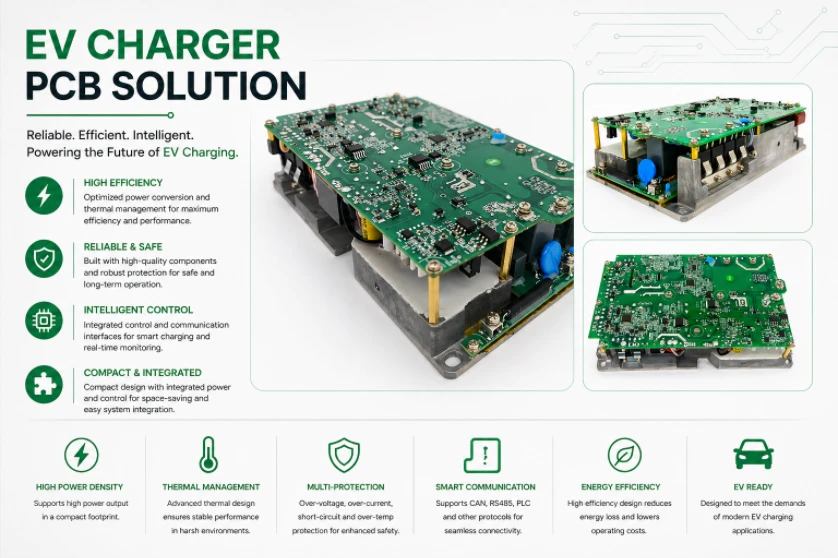
An RFID reader PCB for an EV charger is the contactless-credential interface that captures a card or token, passes an identifier or cryptographic result to the charge-point controller and supports an authorization decision. It is an HMI and security subsystem—not the circuit that makes high-voltage charging safe or the backend protocol by itself.
Key Takeaways
- Freeze the credential ecosystem first: 13.56 MHz proximity cards, vicinity cards, UHF tags, contactless payment and ISO 15118 Plug & Charge are different architectures.
- For an HF/NFC reader, tune the complete antenna, matching network, enclosure, metalwork and ferrite together. A free-space PCB measurement is not the released configuration.
- A 50-ohm match is valid for some reader topologies and measurement interfaces, but it is not a universal rule for every IC-to-antenna connection.
- Validate card reading in every charger noise state: idle, contactor switching, power conversion, communications activity, display operation and environmental stress.
- Specify security, offline authorization, test credentials, production tuning limits, traceability and change control in the RFQ.
Table of Contents
- What does an RFID reader PCB do in an EV charger?
- Which contactless technology should the charger use?
- What belongs in the RFID reader architecture?
- How should a 13.56 MHz reader antenna be designed and tuned?
- How should charger noise and power integrity be controlled?
- How should RFID authentication security be partitioned?
- How should outdoor mechanics and environment be handled?
- Which manufacturing evidence should be required?
- Common RFID reader PCB failure modes
- RFID reader PCB RFQ checklist
- Frequently asked questions
What Does an RFID Reader PCB Do in an EV Charger?
In a public or fleet charger, the reader normally performs four steps: energize or interrogate a credential, decode its protocol, deliver trusted credential data to the main controller and report the user-interface result. The charge-point controller or backend then decides whether to authorize a session according to its local cache, network policy and account state.
Keep these functions separate:
- RFID/NFC reader: physical contactless link and protocol handling;
- charge-point controller: authorization workflow, user interface and session control;
- OCPP connection: charge point to management-system communication;
- ISO 15118: vehicle-to-charge-point communication, including Plug & Charge when implemented;
- metering and power safety: energy measurement, pilot/proximity handling, contactors, residual-current protection and other safety functions.
TI’s NFC-enabled EVSE reference design demonstrates a 13.56 MHz reader integrated with a charge controller, pilot interface, relay drive and energy metering. It also describes the NFC implementation as basic functionality for development. Treat any reference design as an architecture example, then validate the production charger against its applicable safety, radio, payment and network requirements.
Which Contactless Technology Should the Charger Use?
“RFID” covers incompatible frequency bands, coupling methods and credential models. Selecting a reader IC before defining accepted credentials can force an expensive redesign.
| Technology | Typical charger role | PCB/antenna implication | Main decision risk |
|---|---|---|---|
| ISO/IEC 14443 A/B and NFC-A/B at 13.56 MHz | deliberate tap for access or account identification | magnetic loop antenna, protocol-dependent bandwidth and final-enclosure tuning | assuming a card UID alone provides strong authentication |
| ISO/IEC 15693 / NFC-V at 13.56 MHz | vicinity credential or asset/workflow use where the ecosystem requires it | HF loop with different bandwidth/read-range trade-offs | using a higher-Q design that clips sidebands for other protocols |
| FeliCa / NFC-F | regional or closed credential ecosystems | must be supported by the transceiver and firmware | claiming multi-protocol support without testing all intended data rates |
| UHF RFID, including ISO/IEC 18000-63 ecosystems | fleet, asset or vehicle-tag identification at longer range | radiating antenna, matching and enclosure behavior unlike an HF loop | unintended reads, orientation sensitivity and site-level RF planning |
| EMV contactless payment | open-loop payment acceptance | certified payment architecture, secure handling and approved terminal design | treating a general NFC reader as a payment-certified terminal |
| ISO 15118 Plug & Charge | vehicle credential over the charging communication link | not an RFID antenna function | conflating vehicle authentication with card-tap authorization |
RFID can coexist with app authorization, Plug & Charge and contactless payment. Define which methods are primary, fallback or unavailable offline. Also define whether the reader returns only a token, performs card-side cryptography, stores keys or delegates all trust decisions to a separate secure module.
What Belongs in the RFID Reader Architecture?
A robust reader module normally contains more than an antenna and transceiver.
| Block | Design responsibility | Release evidence |
|---|---|---|
| loop or UHF antenna | field pattern, inductance/impedance, keep-out and mechanical integration | controlled geometry, stack-up and assembled measurement |
| EMC filter and matching network | harmonic control, delivered RF power, target impedance and bandwidth | component values/tolerances plus VNA and waveform results |
| RF front end | protocol, modulation, receiver sensitivity, field control and diagnostics | exact device/revision and validated register configuration |
| MCU or host interface | polling, anticollision, credential framing, watchdog and fault handling | firmware version, interface tests and error logs |
| secure element or protected key boundary | credential authentication and key protection where required | security architecture and provisioning responsibility |
| power tree | converter filtering, low-noise rail, sequencing, brownout and reset behavior | rail noise, startup and transient captures |
| charger interface | UART, SPI, USB, CAN, RS-485 or Ethernet as selected | electrical levels, isolation/ESD design and protocol test |
| user interface | buzzer, LEDs or display feedback without coupling into the reader | state timing and noise-state test |
Place the RF front end, EMC filter and matching parts close to their intended reference points. Keep the antenna current path short and controlled. Digital clocks, display cables, switching converters and communication radios should not cross the antenna keep-out or share an uncontrolled return path with the sensitive receiver.
How Should a 13.56 MHz Reader Antenna Be Designed and Tuned?
HF RFID and NFC use magnetic coupling. The PCB loop, matching components and reader front end form a resonant system whose useful bandwidth must carry the selected protocol’s modulation sidebands. The highest possible Q is therefore not automatically the best result.
TI’s TRF79xxA antenna guide, for example, recommends a final Q around 7–10 for applications combining ISO/IEC 14443 and other common NFC technologies, and permits a higher value for an ISO/IEC 15693-only design. Those are device-family and use-case examples, not universal limits. ST’s direct differential reader front ends use a target matching impedance selected around output power, current and application requirements rather than assuming the coil feed itself is a generic 50-ohm transmission line.
Use this tuning sequence:
- Freeze supported protocols, data rates, card types, minimum operating volume and reader power limits.
- Place the loop in the final mechanical location with the real front panel, fasteners, display, ground planes, cables and nearby metal.
- Measure coil inductance, resistance, self-resonance and impedance with the defined fixture and calibrated analyzer.
- Calculate the vendor-recommended EMC filter and matching network, then populate tuning footprints rather than one irreversible value set.
- Measure resonance, Q/bandwidth, field behavior and protocol waveforms with the complete reader energized.
- Test worst-case cards, orientations, distances, temperatures, supply limits and charger operating states.
- Release production limits and a correlation method, not only nominal capacitor values.
Some vendor reference designs expose a 50-ohm point for a VNA and use a zero-ohm link to isolate the antenna matching network during measurement. That is a practical fixture strategy. Other front ends are measured or matched differently, so follow the selected IC’s application note and protect the analyzer from an energized transmitter.
Metal near the loop produces eddy-current loss and detuning. Ground-plane cutouts, antenna position and ferrite can reduce the effect, but the ferrite itself changes inductance and loss. Tune with the ferrite installed in the finished enclosure. A separate rigid-flex PCB or small antenna daughterboard can simplify placement when the main control board sits behind a metal panel.
How Should Charger Noise and Power Integrity Be Controlled?
The RFID reader consumes little power, but it operates beside contactors, switch-mode supplies, metering circuits, displays, cellular/Wi-Fi radios and—in DC chargers—high-power conversion stages. The correct validation question is not “Does the reader work on the bench?” but “Which charger state reduces field strength, receiver margin or digital stability?”
| Charger state | Coupling mechanism | Reader symptom to log | Measurement or design response |
|---|---|---|---|
| standby/polling | local DC/DC ripple, clock harmonics | elevated noise floor or false wakeups | spectrum/rail measurement, polling and clock review |
| contactor open/close | inductive transient, ground bounce, radiated burst | MCU reset, lost transaction or corrupted interface frame | synchronized rail/reset/RF capture; suppress at source and control return path |
| pilot/proximity activity | cable and control-ground coupling | intermittent reads near connector events | interface-state correlation and common-mode path review |
| low- and full-power conversion | switching harmonics and common-mode current | shorter read distance, receiver errors or detuning | near-field probing, conducted-noise sweep and enclosure-bond review |
| display/touch/LED update | fast digital edges and supply steps | periodic read holes or modulation errors | time-correlated logging, layout/decoupling or update scheduling |
| cellular/Wi-Fi transmit | antenna-to-antenna coupling and rail load step | desense, timeout or host reset | coexistence test, antenna separation, filtering and rail transient capture |
| ESD at user surface | direct/capacitive injection into loop and interface | latch-up, reset or damaged front end | system-level ESD test, controlled discharge path and recovery verification |
Use source filtering and return-path control before adding shields or ferrites indiscriminately. A quiet LDO can help the RF rail, but only if upstream converter noise, grounding, dropout and transient response are understood. Galvanic isolation belongs at interfaces where the charger safety and grounding architecture requires it; it is not automatically needed between every reader and controller.
A multilayer PCB can provide controlled reference and power distribution, but keep copper planes out of the loop’s defined keep-out. At 13.56 MHz, ordinary qualified FR-4 is often suitable; low-loss microwave laminate is not a default requirement for an HF loop.
How Should RFID Authentication Security Be Partitioned?
A successful RF exchange proves that the reader saw a credential. It does not prove that the credential is genuine, authorized or entitled to start a billable session.
- Do not use a visible or easily replayed UID as the only trust factor when cloning would create material risk.
- Define whether authentication occurs on the card, in a secure element, in the charger application or at the backend.
- Protect keys through an agreed provisioning and replacement process; do not embed shared production secrets in ordinary firmware without a threat review.
- Decide what happens when the network is unavailable: reject, use a limited local authorization list, permit a capped session or follow another operator policy.
- Bind authorization logs to reader result, charger identity, connector, time, firmware and backend response without storing unnecessary personal data.
- Keep payment-card acceptance inside the required EMV/payment-security architecture. A multi-protocol NFC transceiver does not make a design payment compliant.
OCPP can transport or manage identifiers and authorization outcomes between the charge point and its management system. ISO 15118 Plug & Charge uses vehicle certificates and a different communication path. The reader PCB should expose clean, authenticated results and diagnostic status without pretending to own these end-to-end protocols.
How Should Outdoor Mechanics and Environment Be Handled?
An outdoor charger can expose the reader region to condensation, water ingress, dust, UV-heated front panels, cleaning chemicals, vandalism and repeated card impact. Validate the module in the complete sealed product because enclosure leakage and surface condensation are system properties.
Maintain antenna geometry under assembly pressure and temperature. Plastic ribs, adhesives, ferrite compression, display frames and metal fasteners can shift tuning between prototype and production. Define adhesive, ferrite grade, thickness, placement tolerance and curing process as controlled parts of the RF design.
Conformal coating may protect electronics but can change parasitic capacitance and make later tuning or repair difficult. Specify antenna/matching keep-outs, coating material and thickness only after measuring the effect. Place ESD discharge paths and chassis bonds so current does not return through the reader IC, MCU reset or communication reference.
Which Manufacturing Evidence Should Be Required?
Production acceptance should correlate manufacturing variation with RF and functional performance.
| Control | Evidence to retain | Why it matters |
|---|---|---|
| loop geometry and stack-up | finished trace/gap, copper, dielectric and revision record | shifts inductance, resistance and repeatability |
| ferrite/enclosure configuration | supplier/grade, thickness, adhesive and placement inspection | changes field loss and tuning |
| matching network | exact part numbers, tolerance, lot and fitted-option record | nominal capacitance alone hides Q and temperature behavior |
| RF response | defined VNA/waveform/field test with fixture calibration and limits | verifies resonance, bandwidth and delivered field at stated reference points |
| assembly process | SPI/AOI plus X-ray where package geometry requires it, reflow and repair record | detects opens, shorts, tombstones and hidden-joint defects |
| credential functional test | approved card/tag matrix, orientation, distance, transaction and error result | proves the intended protocols rather than one golden card |
| charger-state immunity | test state, load, radios, display and environmental condition | reveals coupled-noise failures missed by standalone tests |
| traceability/change control | PCB lot, BOM lots, firmware, tuned option and PCN approval | makes drift and field failures diagnosable |
Do not set production acceptance only by “read range.” Range depends on tag antenna, orientation, reader power, enclosure and nearby conductors. Use a controlled reference credential and fixture, while retaining electrical limits that reveal why a unit passes or fails.
Common RFID Reader PCB Failure Modes
| Symptom | Likely causes | Discrimination check |
|---|---|---|
| works as a bare PCB but not behind the panel | metal/ferrite/plastic detuning, ground-plane coupling or antenna displacement | compare VNA/field data through each mechanical build step |
| one card family works and another fails | unsupported protocol/data rate, excessive Q, waveform or firmware configuration | protocol-specific waveform and credential matrix |
| read range falls only during charging | converter harmonic, common-mode current, rail ripple or enclosure coupling | synchronized RF/rail/noise capture versus power state |
| random reader resets | supply dip, ESD, reset routing, watchdog or host-interface fault | scope power/reset, log reset cause and reproduce user-surface ESD |
| high unit-to-unit variation | antenna etch, dielectric, ferrite placement or matching-part tolerance | correlate VNA results with PCB and component lots |
| unauthorized cloned credential succeeds | UID-only authorization, weak key handling or backend policy | credential/security architecture review and controlled negative tests |
| field failures after coating or sealing change | dielectric shift, contamination, adhesive/ferrite movement or trapped moisture | compare controlled pre/post-process RF and environmental data |
RFID Reader PCB RFQ Checklist
Credential and system definition
- accepted standards, card/tag products, data rates, minimum operating volume and multi-card behavior;
- authorization flow, secure element/key provisioning, offline policy, OCPP/backend interface and ISO 15118 boundary;
- payment-terminal scope, radio-market approvals and product security ownership;
- charger states, power levels, communications radios, display and environmental test matrix.
PCB and mechanical package
- schematic, BOM, Gerber/ODB++ or IPC-2581, drill, stack-up, drawing and controlled antenna geometry;
- front panel, ferrite, metalwork, fasteners, cable/display position and enclosure CAD;
- antenna/matching keep-outs, controlled copper, impedance or inductance targets and tuning footprints;
- coating, adhesive, gasket, cleanliness, ESD/chassis and repair requirements.
Manufacturing and validation
- prototype tuning plan, VNA access/calibration, waveform/field method and production limits;
- approved reference credentials, fixtures, distances/orientations, transaction timing and error logs;
- SPI, AOI, X-ray, programming, functional test and charger-state immunity scope;
- serialization, firmware/BOM traceability, retained samples, raw-data format and change notification.
HILPCB can review the released PCB geometry, matching-component footprints, panelization and assembly/test package, then quote an SMT assembly or turnkey PCB assembly scope. Credential security, radio/payment approval, charger safety, backend authorization and complete EVSE compliance remain with the designated product owner unless explicitly included with approved requirements and fixtures.
Reference Standards and Specifications
- ISO/IEC 14443 series — International Organization for Standardization / International Electrotechnical Commission
- ISO/IEC 15693 series — International Organization for Standardization / International Electrotechnical Commission
- ISO/IEC 18092 — International Organization for Standardization / International Electrotechnical Commission
- ISO/IEC 18000-63 — International Organization for Standardization / International Electrotechnical Commission
- NFC Forum Analog and Digital Specifications — NFC Forum
- OCPP 2.0.1 — Open Charge Alliance
- ISO 15118 series — International Organization for Standardization
- IEC 61851 series — International Electrotechnical Commission
- IEC 61000-4 series — International Electrotechnical Commission
- ETSI EN 300 330 — European Telecommunications Standards Institute
- FCC 47 CFR Part 15 — Federal Communications Commission
Use the revisions and regional requirements applicable to the released charger and target markets.
Frequently Asked Questions
Is every EV charger RFID reader a 13.56 MHz NFC reader?
No. Many tap-card systems use 13.56 MHz proximity or NFC technologies, but some deployments use other HF protocols, UHF tags, payment terminals, apps or ISO 15118 Plug & Charge. The credential ecosystem determines the reader.
Must the antenna trace be exactly 50 ohms?
No. Some reader designs use a 50-ohm matching stage or VNA reference point. Other ICs drive a differential matching network designed for a different target impedance. Follow the selected front end’s documented topology.
What Q factor should a 13.56 MHz reader antenna use?
Use the reader-vendor and protocol requirements. Q trades energy transfer against bandwidth, so the right value changes with supported protocols and data rates. Verify it on the complete enclosure, not from a generic online range.
Does a ferrite sheet always improve read range?
Ferrite can reduce loss caused by nearby metal, but it also changes antenna inductance and loss. Select and tune the ferrite as part of the finished mechanical stack, then confirm temperature and production variation.
Can the RFID UID be used as the charger account credential?
It can be an identifier in a low-risk closed system, but UID-only authorization may be clonable or replayable. Use a threat-based security architecture with cryptographic credentials or protected backend validation where misuse matters.
What files are needed for an RFID reader PCB quote?
Provide the controlled PCB data, BOM, antenna and enclosure geometry, ferrite/coating definition, supported credentials, tuning/test method, charger noise-state matrix, quantities, traceability and security responsibility boundaries.
Validate the Reader Inside the Real Charger
Reliable tap-to-charge behavior comes from one correlated design: the credential protocol, antenna match, metalwork, power state, security policy and production test must agree. Measure that complete system, retain the evidence by revision and lot, and treat every enclosure, ferrite, BOM or firmware change as a potential RF and authorization change.