
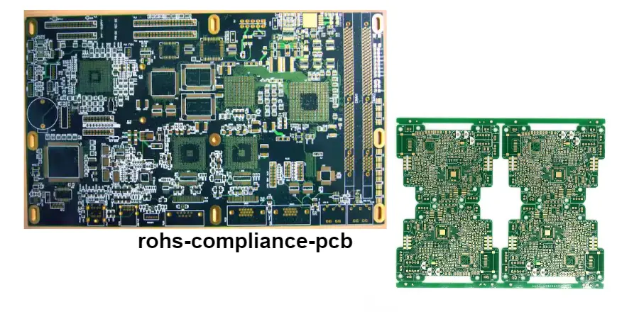
Introduction: why RoHS and REACH are the first lesson in stackup design
Engineers—welcome to the HILPCB Stackup & Materials Academy. Today we won’t start with Dk/Df equations. Instead, we’ll start from something that looks “non-technical” but can decide whether a project succeeds or fails: rohs reach compliance lesson.
Many people treat RoHS (Restriction of Hazardous Substances) and REACH (Registration, Evaluation, Authorisation and Restriction of Chemicals) as a checklist for procurement and legal teams. But for PCB engineers, this is actually the starting point of modern material selection and stackup design. When lead-free solder replaces tin-lead, soldering temperature jumps from ~185°C to >245°C, and the thermal reliability of traditional FR-4 is immediately challenged. That forces us to re-check glass transition temperature (Tg), decomposition temperature (Td), and Z-axis CTE.
So this rohs reach compliance lesson isn’t just about “environmental compliance”. It’s a regulation-driven technology upgrade that directly determines whether your stackup can run reliably under high temperature, high frequency, and high current. It guides the full flow—from material selection to stackup planning to manufacturing validation.
1. Process overview: from design data to finished PCBA
A successful stackup starts with a precise definition of project requirements. It’s not created from thin air—it’s an engineering solution under constraints.
Inputs
- Signal integrity (SI): What is the maximum data rate? (e.g., 10 Gbps PCIe 4.0). This drives Dk/Df requirements and whether you need glass weave skew mitigation.
- Power integrity (PI): What is the maximum operating current? (e.g., 50A). This directly drives copper thickness and high current copper balancing strategy.
- Thermal: What is the power dissipation of key chips? What is the ambient temperature range? This determines whether high-Tg materials or a special thermal reliability stackup (e.g., MCPCB) is required.
- Compliance: What is the application environment? (e.g., industrial, medical). This relates to cti requirement explanation (Comparative Tracking Index) and flame rating (UL94 V-0).
- Physical & Cost: Board thickness limits, layer-count budget, and target cost.
Outputs
- Material list: Specify core (Core) and prepreg (PP) models for each dielectric layer, plus copper foil type (e.g., RTF, HVLP).
- Lamination stack drawing: Layer functions (Signal, GND, Power), dielectric thickness, copper thickness, total thickness.
- Impedance rule table: Trace width/spacing and target impedance for single-ended and differential routing (e.g., 50Ω, 90Ω, 100Ω).
- Manufacturing notes: Special processes such as back-drill depth, resin filling, impedance coupon test requirements, etc.
Core mindset
Stackup design is the process of finding the best balance among performance, cost, and manufacturability. Inputs are your “exam paper”; outputs are your “answer sheet”. HILPCB’s role is to help you make the best trade-offs across all three.
2. Material parameter quick reference: reading a material’s “personality” from numbers
Choosing the right material is half of stackup success. The table below summarizes common HILPCB laminates that meet RoHS/REACH requirements, so you can compare quickly.
📈 HILPCB core laminate performance comparison matrix
Materials insight: When selecting laminates, frequency stability of Dk and consistency of Df define high-speed design quality. For high-power inverters, the CTI value sets creepage margin; for 5G RF, the low-polar molecular structure of Rogers helps reduce skin-effect-related loss.
Parameter notes:
- Dk (dielectric constant): lower is generally better—faster propagation and more stable impedance control. A Dk 3.66 material has ~10% less delay than Dk 4.4.
- Df (dissipation factor): lower is better—especially above 5Gbps, where high Df causes severe attenuation.
- Tg (glass transition temperature): the temperature where the material transitions from rigid glassy state to rubbery state. Lead-free assembly typically requires Tg ≥ 170°C—foundation for thermal reliability stackup.
- CTI (Comparative Tracking Index): surface resistance to tracking under voltage stress. Industrial and HV products often require CTI ≥ 400V (PLC 2) or 600V (PLC 0)—a key cti requirement explanation topic.
3. Core stackup paradigms: evolving from 4 layers to 10+ layers
Once you understand materials, the next step is how to “build” with them. Different layer counts and arrangements serve different applications. Here are classic paradigms.
4-layer: the cost/performance balance point
- Structure: SIG / GND / PWR / SIG
- Use cases: IoT modules, consumer electronics, simple controllers.
- Pros: Low cost and mature process. GND and PWR planes provide return paths and shielding.
- Cons: Impedance control accuracy is limited; high-speed signals are more exposed to crosstalk.
6-layer: the entry choice for high-speed design
- Structure: SIG / GND / SIG / PWR / GND / SIG
- Use cases: Embedded systems, industrial boards with high-speed interfaces (USB 3.0, 1GbE).
- Pros: Two inner signal layers are shielded by GND planes, improving SI/EMI significantly—foundation for reliable high-speed PCB design.
- Key point: Alternate “signal layer ↔ reference plane”.
8+ layer HDI: pushing performance
- Structure: (example) SIG / GND / SIG / PWR / GND / SIG / GND / SIG
- Use cases: Server motherboards, switches, HPC.
- Characteristics:
- HDI: Blind/buried vias free routing space—core content of a full hdi stackup tutorial.
- Power/GND plane pairing: Very low plane inductance for PI.
- Orthogonal routing: Adjacent signal layers route orthogonally (horizontal/vertical) to reduce crosstalk.
| Layers | Typical structure | Core advantage | Use case |
|---|---|---|---|
| 4L | SIG/GND/PWR/SIG | Best cost efficiency | Consumer electronics, simple control |
| 6L | SIG/GND/SIG/PWR/GND/SIG | Strong SI/EMI | Embedded, industrial control, entry high-speed |
| 8L | SIG/GND/SIG/PWR/GND/SIG/GND/SIG | Excellent SI/PI | Servers, communications, data center |
| 10L+ | (multiple SIG/GND pairs) | Peak performance, complex routing | HPC, core networking gear |
4. Golden rules for pairing signal/power/ground and copper thickness
Stackup design is not just “more layers”—it is managing electricity, magnetics, and heat.
- Signal and reference planes: Any high-speed signal layer should be adjacent to a continuous reference plane (GND preferred). This gives the shortest return path, controls impedance, and reduces EMI radiation.
- Power and ground coupling: Tight coupling of power and ground planes (dielectric thickness < 4 mil) forms a natural plane capacitor, providing low-impedance power to high-speed chips.
- High current and copper thickness: For layers carrying >30A, standard 1 oz (35 µm) copper is often insufficient. Use 2 oz (70 µm) or 3 oz (105 µm) Heavy Copper PCB.
- Symmetry: The core of high current copper balancing. The stackup must be symmetric around the center. For example, if L2 is 2 oz, then L(n-1) should also be 2 oz. Asymmetry creates large stress during lamination and reflow and can cause severe warpage.
5. Hybrid lamination and special materials: handling extreme requirements
When a single FR-4 cannot satisfy all constraints, hybrid lamination and special substrates become necessary.
- FR-4 + Rogers hybrid: The most common RF combination. Use Rogers (e.g., RO4350B) on RF signal layers and lower-cost FR-4 for digital/power layers.
- Challenge: Large differences in CTE and lamination parameters; an experienced factory (like HILPCB) is needed to control delamination and reliability risk.
- MCPCB (metal core): Designed for thermal reliability stackup. Aluminum/copper core replaces FR-4, with a thin dielectric to conduct heat quickly to the metal base. Common in high-power LEDs and power modules.
- Flex / rigid-flex: For bendable or dynamic folding applications (wearables, precision medical devices). Main material is polyimide (PI).
| Design type | Core material | Problem solved | Manufacturing notes |
|---|---|---|---|
| RF hybrid | FR-4 + Rogers/Teflon | Balance RF performance and cost | Plasma treatment, dedicated lamination profile |
| MCPCB | Al/Cu core + high-thermal dielectric | Extreme heat spreading | Dielectric withstand voltage, metal machining |
| Rigid-flex | FR-4 + PI | 3D routing, dynamic bending | Coverlay selection, stiffener design |
6. Manufacturing impact: the “last mile” from drawing to real boards
A perfect stackup on paper is still a failure if it can’t be built consistently. Engineers must understand key manufacturing impacts.
🔬 HILPCB core manufacturing matrix for high-speed multilayer PCBs
Lamination cycle and resin rheology
By optimizing Vacuum Lamination parameters, we control resin viscosity dynamics under heat and pressure. This improves Dielectric Thickness uniformity and prevents impedance jumps caused by uneven resin flow and copper pattern density.
Glass weave effect mitigation
For 10Gbps+ differential links, we provide dedicated Skew Mitigation strategies. Use Spread Glass or implement Zig-zag Routing to reduce phase offset caused by glass weave gaps.
TDR impedance measurement validation
Every lot includes Impedance Coupon test strips. We use high-precision TDR to measure differential networks, keep impedance within tight tolerance, and provide a shipment TDR report.
7. HILPCB: your dedicated stackup design partner
From understanding the deeper meaning of rohs reach compliance lesson, to mastering parameters, to balancing performance and manufacturability—stackup design is system engineering. HILPCB is not only a manufacturer, but also your technical partner.
- 200+ in-stock materials: From standard FR-4 to special laminates like Rogers and Taconic, across major global suppliers—so you can choose materials without high MOQ and long lead times.
- Fast stackup proposal service: Provide core requirements (layer count, data rate, thickness), and our engineers deliver an optimized, DFM/DFA-validated stackup within 24 hours, plus detailed impedance calculations.
- In-house testing and validation: We operate labs for impedance test, thermal shock, and CAF (conductive anodic filament) to ensure every HILPCB stackup has strong thermal reliability stackup performance.
Still struggling with stackup design?
Send us your requirements and let HILPCB’s experts build a stackup that balances performance and cost. Upload your Gerber files or contact our online engineers to start a fast and reliable PCB manufacturing journey.
Get a free stackup proposal nowThat concludes today’s rohs reach compliance lesson. Hopefully this class helps you see that stackup design is not just “layer stacking”—it’s a deep understanding and trade-off across materials, regulations, and manufacturing processes. At HILPCB, we turn that complexity into practical engineering services you can use.
Conclusion
This article uses rohs reach compliance lesson as the main line to explain material parameters, stackup planning, impedance/thermal/cost trade-offs, and manufacturing notes—with tables and examples to help teams build a standard stackup library and control risk across design, materials, and test. If you follow the checklists and process windows and involve HILPCB’s DFM/DFA team early, you can accelerate prototype and volume delivery while maintaining quality and compliance.
For manufacturing and assembly support, contact HILPCB Turnkey Assembly or SMT Assembly for DFM/DFT suggestions.
Common Questions
Why are RoHS and REACH important when choosing PCB stack-up materials?
They affect which laminates, prepregs, finishes, and process chemicals can be used in a compliant product. Compliance is not only about the bare board material but also about declarations, traceability, and the full supply chain behind the stack-up.
Does compliance automatically guarantee good electrical or thermal performance?
No. A compliant material still has to meet the signal, thermal, and reliability requirements of the design. Engineers need to balance regulatory status with dielectric properties, copper structure, thickness control, and manufacturing stability.
When does a stack-up need special materials instead of standard FR-4?
That usually happens when the design must support high-speed signals, RF performance, heavy current, extreme heat, or repeated bending. In those cases, hybrid laminates, metal-core materials, or rigid-flex constructions may be more suitable than standard FR-4 alone.
What is the practical benefit of involving the manufacturer early in stack-up planning?
Early discussion helps confirm material availability, impedance capability, lamination limits, and compliance documentation before the layout is locked. That reduces redesign risk and improves the chance of first-pass success in prototype and production.