
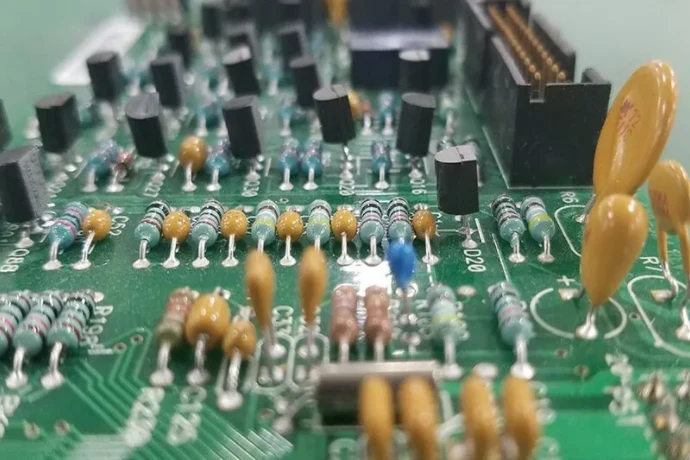
- Selective wave soldering is usually the right choice when a board mixes reflowed SMT parts with a smaller number of through-hole or high-mass components that still need soldering.
- On power and cooling PCBs, the first review point is not the machine setting. It is whether pad geometry, component spacing, thermal relief, pallet access, and solder-joint inspection paths were designed for the process.
- If the board contains bulky inductors, connectors, transformers, high-current terminals, or mechanically loaded through-hole parts, selective wave soldering is often easier to control than full-wave soldering or manual soldering.
- Process success depends on design and manufacturing staying aligned. A layout that ignores nozzle access, shadowing, solder-thieving, or fixture support usually creates instability during pilot builds.
- Validation should close the loop from DFM review to first-article inspection, solder-joint inspection, electrical test, and any downstream coating or environmental-protection steps.
Selective wave soldering is a targeted soldering process for through-hole joints on mixed-technology PCBs. It is most useful when SMT parts are already reflowed, but connectors, transformers, inductors, or terminals still need controlled through-hole soldering without exposing the whole assembly to a second broad thermal cycle.
Contents
- What to review first on a power or cooling PCB
- Key process and design rule table
- Four early risk signals before pilot build
- When selective wave soldering is the better choice
- What design and fixture details decide process stability
- How to inspect and validate the soldering result
- How selective wave soldering affects downstream coating and reliability
- FAQ
- Next steps
- References
- Author and review
What to review first on a power or cooling PCB
For power-conversion, VRM, inverter, fan-control, and cooling-system PCBs, selective wave soldering is not simply a replacement for hand soldering. In engineering terms, it is a controlled process for mixed assemblies where solder-joint quality, thermal exposure, and mechanical repeatability all matter. It does not mean "any through-hole part can be soldered automatically," and it does not solve weak pad design, poor spacing, or inaccessible joints by itself.The first items to review are usually:
- Which through-hole parts still need soldering after SMT reflow
- Whether those parts are electrically critical, mechanically loaded, or thermally massive
- Whether the pad, hole, and copper geometry will wet consistently during localized soldering
- Whether the pallet and nozzle can access the joint without damaging adjacent parts
- Whether the finished joint can still be inspected, tested, cleaned, and protected
Key process and design rule table
| Rule / Parameter | Recommended judgment method | Why it matters | How to verify | If ignored | | --- | --- | --- | --- | --- | | Process fit | Check whether the board is mixed SMT + THT and whether only local joints need soldering | Selective wave soldering is strongest when localized heat and joint targeting are required | Review assembly flow and component list during DFM | Wrong process choice creates unstable joints or unnecessary thermal exposure | | Through-hole component type | Separate connectors, inductors, transformers, terminals, and tall mechanical parts into a dedicated review set | Different mass, pin geometry, and shielding conditions change wetting behavior | Review BOM, drawings, and assembly orientation | A single generic setup often fails across all THT joints | | Pad and hole design | Confirm annular ring, hole finish, thermal relief, and surrounding copper balance | Joint fill and wetting consistency depend heavily on pad and heat-flow behavior | Gerber review, pad-library review, pilot coupon or first article | Cold joints, insufficient fill, bridging, or poor repeatability | | Nozzle and pallet access | Check keep-out area, neighboring SMT height, board underside clearance, and support requirements | The machine can only control what it can physically reach and support | DFA review and pallet design review | Shadowing, missed joints, collision risk, warped board support | | Inspection path | Decide in advance how joints will be inspected after soldering | Some joints are hard to rework or hard to see once assembly continues | Define AOI, X-ray, visual, ICT, or FCT path in the process plan | Defects escape until later functional or field failure | | Downstream protection | Review whether washing, drying, baking, or conformal coating will follow | Flux residue and coating compatibility matter for long-term reliability | Build the post-solder cleaning and protection sequence into NPI | Good joints can still fail later because residue or coating trapped contamination |Four early risk signals before pilot build
When selective wave soldering is the better choice
Selective wave soldering is usually preferred when the assembly already passed SMT reflow, but some through-hole joints still need tighter control than manual soldering can provide. For power and cooling boards, that often includes:- high-current terminals
- press-fit alternatives that are still soldered
- large electrolytic or polymer capacitors
- transformers and magnetics
- tall connectors
- mechanically loaded headers
Compared with full-wave soldering, selective wave soldering reduces unnecessary board-wide reheating and lowers the risk of disturbing nearby SMT parts. Compared with manual soldering, it usually offers better repeatability once the board, pallet, and program are stable.
It is not always the best choice. If the board is mostly through-hole with few SMT restrictions, or if the part geometry is fundamentally hard for nozzle access, another assembly route may be better. That decision should be made during PCB prototype planning and assembly DFM review, not after layout freeze.
For projects that combine high-current board fabrication with mixed-technology assembly, it is often useful to align the PCB structure and assembly route together against through-hole assembly and turnkey assembly capability before the first pilot run.
What design and fixture details decide process stability
Most selective wave soldering failures start in design, not on the machine. The solder nozzle, fluxer, and preheater can only operate inside the geometry they are given. On power boards, three areas usually dominate the outcome.1. Pad, hole, and copper behavior
Pads tied to large planes, heavy copper regions, or heat-spreading structures can pull heat away from the joint. If thermal relief strategy and copper balance are weak, wetting becomes inconsistent from one joint type to another. This is especially relevant on heavy copper PCB and high-thermal PCB designs where thermal behavior is part of the board's core function.
2. Component spacing and access
Adjacent SMT parts, shielding cans, tall parts, and connectors can block nozzle movement or create shadowing. A board may be electrically correct and still be awkward to solder. That is why component placement, underside clearance, and keep-out rules need to be part of the same review as the assembly process.
3. Pallet support and board stability
Power and cooling assemblies often include thick boards, uneven mass distribution, or heavy through-hole parts. Without good fixture support, localized heating and solder contact can create board movement or inconsistent joint geometry. Pallet design is not an afterthought. It is part of process capability.
For mixed-technology boards that also need SMT assembly, these decisions should be treated as one assembly system, not as two isolated steps.
How to inspect and validate the soldering result
Selective wave soldering should be validated as a process, not just as a visual appearance check. A stable validation path usually combines:- DFM and DFA review before build
Confirm part type, pad structure, spacing, fixture concept, and inspection route before pilot release. - First-article inspection after pilot soldering
Check joint appearance, wetting behavior, hole fill, orientation, and any obvious thermal or collision issue. - Electrical test
Use ICT, FCT, or other project-specific verification to confirm the joint is electrically sound in the assembled product. - Defect review and process feedback
Compare defects by joint family, not just by board count. Connectors, magnetics, and terminals often need different corrective actions. - Release decision for volume production
Freeze the approved fixture, inspection path, cleaning path, and rework boundary before scaling the job.
Inspection should fit the actual risk. Visual inspection may be enough for accessible joints, but hidden or mechanically critical joints may need a stronger verification path. IPC's through-hole acceptability guidance is commonly used as the inspection reference, while the soldering-material and process side is usually aligned with the J-STD family of requirements.
How selective wave soldering affects downstream coating and reliability
On many power and cooling products, the soldering step is not the end of the risk chain. Boards may still go through cleaning, drying, conformal coating, enclosure assembly, or environmental sealing. That means selective wave soldering must be evaluated together with what comes next.The most common downstream interactions are:
- residue left in difficult-to-clean zones around through-hole joints
- coating trapped around poorly cleaned pins or solder fillets
- rework difficulty increasing sharply after coating
- thermal cycling and vibration loading at connectors or tall parts
If the finished board will later receive box-build assembly or environmental protection, the solder-joint review should include the downstream process boundary from the beginning. If coating is part of the product path, the process team should also decide early whether PCB surface finish choice, cleaning method, and coating chemistry are all compatible with the assembly route.
FAQ
When should a power PCB use selective wave soldering instead of manual soldering?
Use it when the assembly includes repeated through-hole joints that need better repeatability, controlled localized heating, and lower operator dependence than manual soldering can provide.
Is selective wave soldering only about machine settings?
No. Pad design, copper balance, component spacing, pallet support, and inspection planning usually decide whether the machine settings can work consistently at all.
Which parts on a cooling or power board most often trigger selective-wave review?
High-current terminals, connectors, large capacitors, magnetics, transformers, and other through-hole parts with high thermal mass or mechanical load usually need the earliest review.
Can selective wave soldering reduce risk to nearby SMT parts?
Often yes. Because the process targets local joints instead of exposing the entire board to broad heating again, it can be easier to control on mixed SMT + THT assemblies.
What should be frozen before releasing the process to volume production?
Freeze the approved layout assumptions, pallet concept, soldering route, inspection method, electrical-test path, cleaning path, and any downstream coating or protection constraints.
Next steps
If your board mixes reflowed SMT parts with connectors, terminals, magnetics, or other through-hole joints, the most useful next step is usually not asking for a generic process recommendation. It is reviewing the actual board stack-up, part geometry, and assembly flow together.HILPCB can support that review through:
- Through-hole assembly evaluation for mixed-technology boards
- SMT assembly and process alignment when the product combines reflow and selective soldering
- Turnkey assembly review when fabrication, assembly, inspection, and downstream protection need to be coordinated
- PCB prototype support if you want to validate the soldering route before committing to larger volume
- Request a quote when you already have Gerber, BOM, and assembly requirements ready for review
If you are still deciding whether a power or cooling board should use selective wave soldering, manual soldering, or a different assembly route, a pre-review before pilot build usually saves more time than tuning the process after defects appear.