
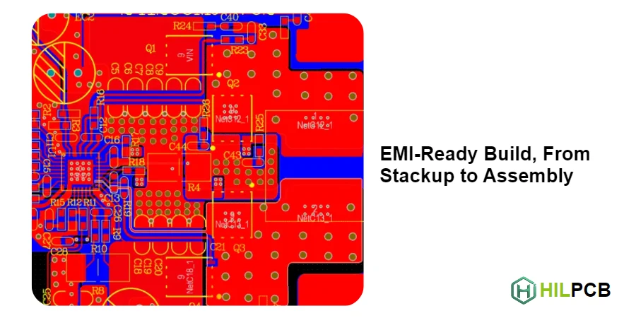
Shielding provides the final layer of defense against electromagnetic interference when design techniques alone cannot achieve required EMI levels. At high frequencies, effective shielding requires understanding the physics of electromagnetic containment and careful attention to implementation details that determine whether shields work as intended or become part of the problem.
This guide provides practical knowledge for implementing effective shielding in high frequency PCB designs, from shield physics through manufacturing considerations that deliver the containment performance your application requires as part of comprehensive EMI control for high frequency PCB.
HILPCB provides RF circuit board manufacturing with integrated shielding support including shield can footprints, via fence patterns, and edge treatments optimized for high frequency EMI containment.
Shielding Effectiveness Fundamentals
Shielding effectiveness (SE) measures how well a shield attenuates electromagnetic fields. Understanding what determines SE guides material selection and design decisions.
At HILPCB, our engineering team can recommend shielding approaches appropriate for your frequency range and effectiveness requirements during precision fabrication planning.
Shielding Mechanisms
Shields attenuate electromagnetic fields through two primary mechanisms. Reflection occurs at the shield surface where impedance mismatch between air and metal reflects incident energy. Absorption occurs as fields penetrate the metal and energy converts to heat through resistive losses. The total shielding effectiveness combines reflection and absorption contributions.
At low frequencies, reflection dominates for electric fields while magnetic shielding requires high-permeability materials and significant thickness. At high frequencies (above a few MHz), both electric and magnetic fields are effectively shielded by thin conductive barriers, and absorption becomes significant.
Skin Depth Effects
At high frequencies, current flows only in a thin surface layer of the conductor. Skin depth in copper at 1 GHz is approximately 2 μm. Shield thickness beyond a few skin depths provides little additional absorption. This means very thin metal shields are effective at high frequencies—foil thickness is adequate.
Material Selection
Copper and aluminum are common shield materials. Copper offers higher conductivity but aluminum is lighter and cheaper. For most HF applications, the difference is minimal—construction quality matters more than material selection. Steel provides better magnetic shielding at low frequencies but may be unnecessary at high frequencies.
Aperture Dominance
At high frequencies, shield effectiveness is usually limited by apertures (holes, slots, seams) rather than the shield material itself. A perfect shield with a small hole can leak significantly. Aperture control becomes the primary design challenge. Effective shielding supports radiation suppression in HF PCB implementation.
On-Board Shielding Implementation
Shield cans placed directly on the PCB over noise-generating or noise-sensitive circuits provide local shielding without requiring external enclosures.
HILPCB manufactures PCBs with shield can footprints and supporting structures for integrated on-board shielding.
Shield Can Design
Common shield can configurations include stamped metal cans with pick-and-place attachment, two-piece designs with separate fence and lid, and formed sheet metal enclosures. Key parameters include height clearance for components, perimeter contact to ground, and provision for assembly access (removable lid).
The shield perimeter must make continuous contact with the PCB ground plane. Gaps allow field leakage. Contact tabs or continuous contact surfaces ensure reliable connection.
Shield Can Implementation
Ground Plane Interface
The PCB ground plane forms the bottom of the shield enclosure. Ground plane quality directly affects shielding effectiveness. Solid copper beneath the shield area, without cuts or voids, is essential. Signals entering or exiting the shielded area should be filtered or pass through controlled openings.
Via Fence Under Shield Walls
A via fence beneath shield can walls improves high frequency containment. Without the fence, fields can propagate in the dielectric between PCB layers under the shield wall and escape. Via spacing should be λ/20 or closer at the highest frequency of concern. This technique integrates with overall grounding strategy for HF PCB design.
Multi-Compartment Shields
Dividers within shield cans create separate compartments for different circuits. This provides isolation between circuits within the same general shielded area. Each compartment should have its own via fence beneath the divider.
Via Fence and Edge Shielding
Via fences provide shielding without physical metal shields by creating a conductive barrier through the PCB stack.
HILPCB supports dense via fence patterns with spacing appropriate for your frequency requirements.
Via Fence Construction
A via fence is a row of ground vias spaced closely enough to block electromagnetic fields at the frequencies of interest. The fence connects ground planes through the PCB stack, creating a vertical conductive wall. Fields attempting to propagate through the fence are reflected or absorbed.
Spacing Requirements
Via spacing determines the maximum frequency at which the fence is effective. General guideline: spacing should be less than λ/20 to prevent significant leakage. At 10 GHz in FR-4, λ/20 ≈ 0.75mm (30 mils). Closer spacing is required for higher frequencies.
Applications
Via fences serve multiple purposes. Perimeter fences around board edges reduce edge radiation. Fences between circuit sections provide isolation. Fences beneath shield can walls enhance physical shield performance. Channel fences guide routing and prevent crosstalk. These applications support EMI noise reduction in high frequency PCB design.
Edge Treatment
Board edges can radiate from the parallel-plate waveguide formed by power and ground planes. Edge plating (connecting all layers at the edge) reduces this radiation. Via stitching near edges provides similar benefit. Keep high frequency traces away from edges. HILPCB offers PTFE PCB fabrication with edge treatment options for demanding EMI requirements.
Aperture Control and Management
Apertures—any opening in a shield—limit high frequency shielding effectiveness. Managing apertures is often the critical factor in achieving required shielding performance.
Aperture Leakage Physics
An aperture in a shield acts as a slot antenna. Leakage depends on aperture size relative to wavelength. The critical dimension is the longest dimension (length for slots, diameter for round holes). A slot λ/2 long resonates and leaks maximally. Smaller apertures leak less; larger apertures can leak more.
Rule of thumb: keep maximum aperture dimension below λ/20 for good shielding.
Ventilation and Apertures
Equipment needs ventilation but ventilation holes leak EMI. Strategies include many small holes instead of few large holes (same air flow, less leakage), honeycomb vents that provide waveguide-below-cutoff attenuation, and conductive mesh that allows air while maintaining electrical continuity.
Display Windows
Visual displays need transparent openings. Conductive transparent materials include ITO (indium tin oxide) coated glass and fine conductive mesh. ITO provides good transparency with moderate shielding. Mesh provides better shielding but may affect display quality.
Seams and Joints
Shield enclosure seams leak if not properly managed. Continuous contact along seam length is essential. EMI gaskets fill gaps and maintain contact. Gasket selection depends on frequency range, environmental requirements, and assembly method. Finger stock, conductive elastomers, and wire mesh are common gasket types.
Signal Penetrations
Signals entering and exiting shielded enclosures are potential leak points. Filter all signals at the shield boundary. Use filtered connectors or add filtering components at the enclosure wall. Ground shield connections to connector shells.
Enclosure-Level Shielding
System enclosures provide the final shielding barrier between internal electronics and the external environment.
HILPCB supports enclosure integration through proper Rogers material construction and PCB-to-enclosure interface design.
Enclosure Construction
Metal enclosures provide inherent shielding. Die-cast aluminum and sheet metal steel are common. The enclosure must be electrically continuous—all panels connected with low-impedance bonds. Paint and anodize can insulate joints; ensure metal-to-metal contact at critical joints.
PCB-to-Enclosure Integration
Mounting the PCB in the enclosure should maintain shielding integrity. Ground the PCB to enclosure at multiple points. Connect near I/O interfaces for cable shield termination. Use standoffs with low-impedance path to enclosure. Verify that mounting hardware doesn't create isolation between PCB ground and enclosure.
Cable Entry Points
Cables penetrating the enclosure are major potential leakage points. Use shielded connectors with shell bonded to enclosure. Filter signal lines at the enclosure boundary. Keep cable lengths inside the enclosure short. Position cable entries away from sensitive internal circuits.
Testing Considerations
Enclosure shielding effectiveness can be measured. Pre-compliance testing verifies shielding integrity before certification. Near-field probing identifies leakage points. Comparison of emissions with and without enclosure quantifies contribution.
Implementation and Manufacturing Considerations
Proper implementation ensures designed shielding performs as intended. Manufacturing quality and assembly procedures affect final shielding effectiveness.
PCB Manufacturing for Shielding
Shield footprints must be accurate. Ground plane continuity beneath shields is critical. Via fence accuracy affects high frequency performance. HILPCB maintains manufacturing precision for shielding features.
Shield Assembly
Solder attachment of shield cans requires proper thermal management. Reflow attachment is common but hand soldering may be needed for large shields. Shield contact pressure affects performance—spring contact shields require attention to contact force. Removable shields must maintain contact through many removal cycles.
Inspection and Verification
Visual inspection verifies shield presence and placement. Electrical testing can verify ground connection. X-ray may be needed to verify solder joints on hidden contacts. Functional EMI testing confirms effectiveness.
HILPCB Shielding Design Services
HILPCB delivers high frequency PCBs with integrated shielding:
Shield Integration: Shield can footprints, contact pads, and via fences manufactured to specification.
Via Fence Patterns: Dense via arrays with spacing appropriate for your frequency requirements.
Edge Treatment: Perimeter stitching and edge plating options for radiation control.
Design Support: Engineering consultation on shielding approaches and implementation for your EMI requirements.
From prototype development through volume production, HILPCB provides shielding-ready high frequency PCBs.
Contact HILPCB for shielding design review and manufacturing quotation.