
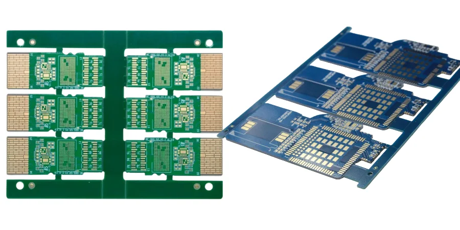
With explosive growth in AI, ML, and HPC, data-center bandwidth demand is rising at a breathtaking pace. Traditional architectures that rely on pluggable optical modules are hitting physical limits in signal attenuation, power, and port density. In this context, Co-packaged Optics (Co-packaged Optics, CPO) has emerged: by packaging the optical engine and the switch ASIC on the same baseboard, it dramatically shortens the electrical path and reduces power and latency. But this disruptive architecture also brings unprecedented challenges to PCB design, fabrication, and assembly—especially the SMT assembly process.
As an engineer focused on electro-optical interconnects and thermal design for CPO baseboards, I know CPO success is not just a win for chips or optics—it’s the result of system-level co-engineering. The PCB baseboard that carries the electro-optical conversion core sits at the center, and its SMT assembly process combines cross-disciplinary problems in high-speed circuits, precision optics, and complex thermal management. This article explores the core SMT assembly technologies for data-center optical-module PCBs in the CPO era, highlighting key challenges and practical solutions in electro-optical co-design, thermal-power management, and precision manufacturing.
CPO board-level interconnect challenges: from SI to electro-optical interface co-design
The core advantage of CPO is reducing the high-speed electrical link length from tens of centimeters (ASIC to front panel) to just a few centimeters (ASIC to an optical engine on the same baseboard). That shift creates new requirements for PCB interconnect design.
High-speed signal integrity (SI)
In CPO systems, the ASIC and optical engine typically communicate through 56G/112G PAM4 links. At these data rates, even small impedance discontinuities, crosstalk, or loss can drive the bit error rate (BER) sharply higher and impact system performance. PCB design must follow the strictest SI principles—covering precise differential impedance control (typically 90Ω or 100Ω), plus careful optimization of vias, connector transitions, and the BGA fanout region.
In practice, we often draw on low-loss QSFP-DD module PCB experience, but CPO requirements are even tighter. Material selection is critical—for example, Panasonic Megtron 6/7, TUC TU-883/933+, or ultra-low-loss dielectric materials from Rogers/Isola to minimize attenuation. Back-drilling removes unused via stubs, and optimized anti-pad design reduces via capacitance to further protect SI. At HILPCB, we use advanced simulation tools (such as Ansys HFSS) to model and optimize every critical high-speed channel, ensuring sufficient eye opening (Eye Diagram) margin.
Co-design of electro-optical interfaces
Unlike conventional PCBs, CPO baseboards must handle both electrical and optical signals. During layout and routing, precise space and location must be reserved for fiber array access. This often requires dedicated cavities or windows in the PCB so a fiber array unit (FAU) can be aligned precisely to the optical engine’s grating coupler (Grating Coupler) or edge coupler.
This co-design demands extremely tight dimensional control from the PCB manufacturer. Across the full Co-packaged optics baseboard manufacturing flow—from lamination and drilling to final routing—tolerances must be tightly managed so fiber alignment stays at the micrometer level. Any deviation can cause severe optical coupling loss and render the module unusable.
Thermal management: CPO power distribution and system-level cooling strategies
Power is another major CPO challenge. In a typical CPO switch system, ASIC power can exceed 500W, while multiple surrounding optical engines can add more than 100W. Concentrating that heat into a small area creates very high heat flux density and stresses the cooling system.
Power distribution and thermal budget
CPO thermal design must start at the system level. First, you need an accurate power map of the ASIC and optical engines and a detailed thermal model. Optical engines are temperature-sensitive; temperature variation can shift laser wavelength and degrade link quality. Optical engine operating temperature typically must be held within a defined range (e.g., 70–85°C), while ASIC junction temperature should remain below 100°C.
This requires differentiated cooling capability. Usually, a large high-performance heat sink (Heat Sink) or vapor chamber (Vapor Chamber) directly covers the ASIC to remove most of the heat. Optical engines may need independent, finer cooling paths. In Co-packaged optics baseboard manufacturing, the PCB itself also becomes part of the thermal path: embedding Heavy Copper PCB layers or designing dense thermal vias (Thermal Vias) can efficiently conduct heat from the die underside to the opposite PCB side or to external cooling structures.
Advanced cooling structures
Traditional air cooling is increasingly insufficient for CPO heat flux. Liquid cooling (Liquid Cooling) is becoming the mainstream approach. By integrating microchannels into the heat sink, coolant can flow directly over the heat source and remove heat with high efficiency. This means PCB design must closely coordinate with the liquid-cooling module’s channels, inlet/outlet ports, and sealing structure. In more advanced concepts, microchannels are integrated directly into the PCB baseboard or package substrate—so-called “board-level liquid cooling”.
Key points for CPO thermal management
- Differentiated cooling: Design independent cooling paths for the ASIC and optical engines to meet different temperature-control requirements.
- Low thermal-resistance path: Optimize every step from die to heat sink, including TIM (thermal interface material), PCB thermal vias, and baseboard materials to minimize total thermal resistance.
- System-level integration: PCB design must be tightly integrated with the cooling module (air or liquid) to ensure mechanical compatibility and thermal performance.
- Temperature monitoring: Integrate multiple temperature sensors on the PCB to monitor critical hot spots in real time and enable closed-loop thermal management.
Materials and stack-up design: low-CTE baseboard reliability and warpage control
CPO modules are typically large and integrate multiple materials—silicon ASICs, InP/SiPh optical engines, organic PCB baseboards, and metal heat sinks. These materials have significantly different coefficients of thermal expansion (CTE). During thermal cycling such as reflow in SMT assembly, CTE mismatch can generate large internal stress and cause PCB warpage (Warpage).
CTE mismatch and warpage challenges
Warpage is the number-one killer for CPO assembly. Severe warpage can cause BGA opens or cracked joints—especially under massive ASIC packages with tens of thousands of balls, where a single defect can scrap the entire module. Warpage also affects alignment accuracy between the optical engine and the fiber array.
To address this, PCB material selection and stack-up design (Stack-up) are critical. We prioritize low-CTE core materials and use symmetric stack-up structures to balance internal stress. In extremely demanding applications, ceramic substrates or low-CTE metal-core baseboards (such as CIC or CMC) may be used—such as Metal Core PCB—to improve dimensional stability. This level of material/structure control is an extension and upgrade of high-end QSFP-DD module PCB manufacturing experience.
Reliability and hybrid lamination
CPO modules must operate reliably in data-center environments for long periods (often >7 years), so reliability is paramount. Beyond warpage control, you must also consider long-term heat resistance, moisture resistance, and electro-migration resistance. Complex CPO baseboards often integrate high-speed signal layers, power layers, and optical-path layers, which may require hybrid lamination (Hybrid Lamination)—bonding different dielectrics (e.g., FR-4 and Rogers) to balance cost and performance. This places high demands on the PCB manufacturer’s lamination process control.
Precision assembly flow: fiber-array alignment and curing processes
The CPO SMT assembly flow is far more complex than conventional PCB assembly, with the core challenge being precision alignment and fixation of the fiber array.
Sub-micron alignment
Single-mode fiber cores are only ~9 μm in diameter. To achieve efficient optical coupling, the fiber array output must align to the optical engine’s grating couplers or waveguides with sub-micron (<1 μm) accuracy. Achieving this requires high-precision automated alignment equipment.
Alignment is typically done via passive or active alignment. Passive alignment relies on high-precision mechanical features, such as V-grooves etched into silicon to locate fibers. Active alignment is performed under live optical power: the system monitors optical power in real time and dynamically adjusts the fiber-array position (six degrees of freedom: X, Y, Z, Pitch, Yaw, Roll) until maximum coupling efficiency is reached.
Fixtures, curing, and practical challenges
During alignment and fixation, dedicated assembly fixtures (Fixture) are critical. They must rigidly hold the PCB baseboard and optical components while preventing displacement from thermal expansion/contraction during curing.
Once the optimal position is found, low-shrink, high-reliability UV-curable or heat-curable adhesive is used for permanent fixation. The curing process itself is challenging: adhesive shrinkage can cause tiny position shifts and reduce optical power. Therefore, adhesive properties, dispensing, and curing profiles must be tightly controlled. For fast-delivery Co-packaged optics baseboard quick turn projects, a mature, repeatable alignment-and-curing process is a key success factor.
HILPCB CPO assembly strengths
- High-precision placement: Advanced SMT lines capable of handling large baseboards and precision optical components, with placement accuracy down to ±15 μm.
- Automated optical alignment: A 6-axis active-alignment platform enabling sub-micron fiber-array-to-chip alignment for optimal coupling efficiency.
- Controlled curing process: Precision dispensing systems and programmable UV/thermal curing equipment to minimize displacement caused by cure shrinkage.
- DFM/DFA expertise: Engineering involvement early in design to advise on fixture design, tolerance allocation, and assembly flow.
Test and validation: key steps to ensure CPO system performance and reliability
After complex assembly, comprehensive and rigorous testing is the last—and most critical—line of defense to ensure CPO functionality, performance, and reliability. Test flows typically include electrical tests, optical tests, and system-level validation.
Electrical and optical performance tests
Electrical tests focus on high-speed link quality. We use a vector network analyzer (VNA) and time-domain reflectometer (TDR) to check insertion loss, reflection, and impedance continuity. High-speed oscilloscopes and bit error rate testers (BERT) are used to evaluate PAM4 eye quality and BER performance.
Optical tests include measuring per-channel output power, center wavelength, spectral width, and extinction ratio (ER). These parameters directly affect optical transmission quality. On the receiver side, sensitivity testing is key—it determines the minimum optical power the module can demodulate correctly. Here, a detailed TIA/LA receiver board checklist becomes especially important. This checklist guides test items for transimpedance amplifiers (TIA) and limiting amplifiers (LA), and its rigorous testing mindset extends throughout CPO receiver-module validation. We ensure every receive channel is evaluated thoroughly to guarantee stable performance across operating conditions.
System-level validation and CMIS
Finally, the CPO module must be validated in an environment close to real use. This includes installing it on a test board and running loopback (Loopback) tests to confirm correct TX/RX behavior across all channels. You also need to verify compliance with CMIS (Common Management Interface Specification) so the host system can read module information, monitor status (e.g., temperature, optical power), and perform necessary control. A complete TIA/LA receiver board checklist can also support calibration of receiver-related monitoring parameters in CMIS (such as RSSI).
At HILPCB, we provide a one-stop SMT assembly service covering DFM analysis, component sourcing, precision assembly, and comprehensive functional testing—so every delivered CPO module has passed strict quality inspection.
HILPCB CPO manufacturing and assembly capabilities
Mastering CPO complexity requires deep technical accumulation and advanced manufacturing platforms from both PCB makers and assembly service providers. With years of focus in high-speed communications—especially experience in low-loss QSFP-DD module PCB and complex IC substrate PCB—HILPCB is ready for the CPO era.
Our Co-packaged optics baseboard manufacturing capabilities cover the full flow from material selection and stack-up design to precision circuit fabrication and final dimensional control. We can support ultra-large boards, very high layer counts (>30L), mixed-dielectric lamination, and embedded passive/active components.
On the assembly side, we provide not only standard SMT assembly, but also the high-precision optical assembly required by CPO. Our prototype assembly service supports fast Co-packaged optics baseboard quick turn to accelerate R&D cycles. Our engineering team applies a rigorous methodology—similar to a TIA/LA receiver board checklist—throughout manufacturing and test workflows to ensure every step meets the highest standards.
HILPCB CPO manufacturing capability overview
| Item | Capability |
|---|---|
| Max layers | 64L |
| Supported materials | Megtron 6/7/8, Tachyon 100G, Rogers, Isola, low-CTE materials |
| Min trace/space | 2/2 mil (50/50 μm) |
| Max board thickness | 12 mm |
| Impedance tolerance | ±5% |
| Surface finish | ENIG, ENEPIG, Immersion Silver, OSP, etc. |
Conclusion
In summary, Co-packaged Optics (CPO) is reshaping the future of data-center interconnects. But realizing that progress depends heavily on synchronized evolution in PCB manufacturing and assembly. In the CPO era, SMT assembly goes far beyond traditional electronics assembly—it is a system engineering effort that deeply integrates high-speed circuit design, thermodynamics, materials science, and precision optics. From managing sub-micron alignment tolerances, to controlling hundred-watt heat flux, to protecting multi-10G signal integrity, every step is challenging.
As your partner, HILPCB is committed to providing a one-stop solution—from design optimization and PCB manufacturing to final precision assembly—to help you overcome the barriers on the path to CPO productization. We believe that through close collaboration and continuous innovation, we can jointly manage the complexity introduced by CPO and drive next-generation data-center technology forward. Choosing a professional SMT assembly partner is the cornerstone of CPO project success.
Common Questions
Why is SMT assembly harder for data-center optical modules?
It must control high-density electrical and optical interfaces, tight thermal budgets, and very small alignment tolerances in one manufacturing flow.
What risks are most critical in CPO builds?
Warpage, fiber-array misalignment, solder voiding, and signal-loss issues around 56G and 112G PAM4 channels are common early risks.
Which validations should be included before volume ramp?
FAI, flying probe test, and staged NPI work across EVT, DVT, and PVT help catch assembly and reliability issues before mass production.
How does the right manufacturing partner help?
A partner with electro-optical co-design experience, low-CTE material control, and precision curing and alignment capability can reduce iteration time and yield loss.