
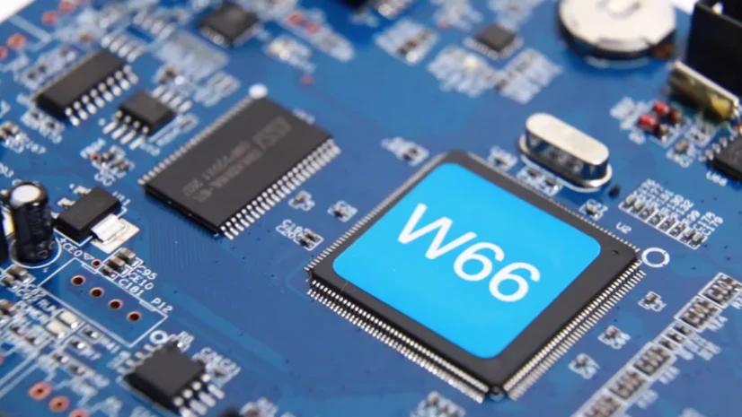
With data centers, AI, and 5G communication advancing at unprecedented speed, required data rates have jumped from 28G/56G to 112G—and are moving toward 224G. In these ultra-high-speed links, PCB is no longer just a carrier for components; it is a critical part of the signal channel. Every pad, every trace, and every via directly affects signal integrity. In this precise and complex ecosystem, SMT assembly is decisive. It is no longer a simple “soldering step,” but the last—and most critical—line that turns design intent into physical reality and protects high-speed signals from loss and distortion.
A great SMT assembly process must deeply understand high-speed signal physics—from impedance matching and crosstalk control to return loss. Even tiny deviations—slight solder paste volume changes or micron-level placement offsets—can be amplified in high-speed channels and cause performance degradation or failure. That’s why choosing a partner with both SI expertise and top-tier manufacturing capability matters. Highleap PCB Factory (HILPCB) provides an end-to-end solution from design optimization to final test, helping ensure your advanced products don’t compromise on performance. Our Turnkey PCBA service is designed to simplify your supply chain so you can focus on core innovation.
What role does SMT assembly play in high-speed SI?
Traditionally, SMT assembly is “just” about accurately soldering components onto PCB. But in high-speed digital systems, the meaning goes far beyond that. It directly impacts the electrical performance of the entire channel and often determines whether SI and PI succeed or fail.
First, impedance continuity is the lifeline of high-speed transmission. In PCB design, engineers use simulation tools to target differential impedance (e.g., 90Ω or 100Ω). But during SMT assembly, pads, solder joints, and component leads become part of the transmission line. Solder joint geometry, paste volume/chemistry, and component alignment all influence local impedance. For example, excess solder increases parasitic capacitance and lowers impedance, causing reflections and higher insertion loss. For high-speed connectors like SFP/QSFP-DD, impedance control around the pin field is extremely tight—small assembly deviations can break carefully engineered “Launch Tuning.”
Second, placement accuracy directly affects timing and crosstalk. For high-speed differential pairs, the two traces must maintain strict length matching and symmetry to suppress common-mode noise. If passives (e.g., coupling capacitors) or active devices (e.g., SerDes) rotate or shift slightly during placement, symmetry breaks, skew increases, mode conversion rises, and eye diagrams degrade.
Finally, solder joint quality determines long-term reliability. Voiding under BGA is a persistent challenge in high-speed designs. Voids reduce mechanical strength and thermal performance, and can also change electrical behavior at high frequency. A professional SMT assembly process uses optimized reflow profiling and strict X-Ray inspection to keep voiding within IPC limits and maintain stable signal performance.
Why is DFM/DFT/DFA review the foundation of high-reliability assembly?
In any complex engineering project, prevention beats rework. In high-speed PCB fabrication and assembly, that principle is embodied by DFM/DFT/DFA review—Design for Manufacturability (DFM), Design for Testability (DFT), and Design for Assembly (DFA). Together they bridge design and manufacturing to ensure the product moves smoothly from drawings to shipment.
DFM (Design for Manufacturability): focuses on bare-board manufacturing feasibility—line/space, via design, stackup, etc.—to deliver high yield and low cost. For high-speed boards, DFM emphasizes impedance tolerance, backdrill depth accuracy, and surface finish impact on loss.
DFA (Design for Assembly): focuses on SMT assembly. It checks whether placement is reasonable (e.g., avoiding “shadowing” of small parts by tall parts during reflow), pad designs meet IPC to prevent tombstoning/bridging, and there is enough spacing for BGA rework and inspection.
DFT (Design for Testability): ensures the assembled PCBA can be tested efficiently and comprehensively. This includes test points, probe access for ICT, and integrating Boundary-Scan/JTAG chains so dense IC pins can be tested without physical probes.
A thorough DFM/DFT/DFA review catches risks early and avoids costly late changes or delays. For example, DFA can recommend NSMD pads for more reliable BGA joints; DFT can ensure critical nodes are accessible via JTAG to simplify bring-up. HILPCB provides a free and in-depth DFM/DFT/DFA review service, working closely with your design team and protecting your High-Speed PCB project from a manufacturing and assembly perspective.
⚙️ SMT Assembly precision manufacturing optimization flow
End-to-end parameter monitoring and closed-loop feedback enable stable assembly of 01005-class components with low-void control.
Assess pad openings, component spacing, and stencil fit to reduce shorting and tombstoning risks at the source.
Nano-coated stencils plus in-line SPI monitoring keep print thickness deviation below 10%.
Multi-point recognition and vision compensation deliver micron-level alignment for dense parts like BGA/QFN.
KIC real-time profiling enables dynamic optimization in nitrogen to suppress solder voiding.
3D AOI plus 2.5D X-Ray covers solder wetting and hidden BGA internal defects.
Precision solder paste printing: the first quality gate for high-speed PCBA
If SMT assembly is a precision building, solder paste printing is the foundation. Industry data shows over 60% of SMT defects originate from paste printing. For high-speed PCBA, print quality directly determines solder joint reliability and electrical performance.
Stencil design is step one. Stencil thickness, aperture shape, and aspect ratio must match component types and pad sizes. For 0.4mm-pitch BGA or 01005 passives, laser cutting plus electropolishing helps ensure clean release and consistent deposits.
Solder paste selection is just as critical. Paste combines alloy powder and flux. Powder particle size (e.g., Type 4/Type 5) and flux activity influence print quality and soldering behavior. In high-speed applications, low-residue, halogen-free no-clean flux is often preferred to avoid negative effects on high-frequency signals.
Process control ensures consistency. Modern printers + SPI (Solder Paste Inspection) enable automated print/clean and 2D/3D inspection. Real-time monitoring of volume/area/height/offset per pad catches defects early and prevents escapes. For high-speed differential-pair pads, even small paste variations can introduce impedance discontinuities.
How does the reflow profile affect performance and lifetime of high-speed devices?
After paste printing and placement, PCBA enters reflow soldering—the key thermal process that forms reliable joints. The reflow profile is a carefully designed curve with four main zones:
- Preheat: slowly ramps (typically 1–3°C/s) from ambient to ~150°C to activate flux and reduce thermal shock.
- Soak: holds around 150–200°C for ~60–120s to equalize temperature and remove oxides.
- Reflow: quickly rises above alloy liquidus (e.g., SAC305 peak ~235–245°C) and stays ~20–40s to form IMC.
- Cooling: controlled cooling (typically ~-4°C/s) solidifies joints; too fast increases stress, too slow can coarsen grains and weaken joints.
For high-speed PCB with large BGA/FPGA or high-power modules, reflow tuning is especially challenging. Large parts and heavy copper areas heat slowly while small parts heat quickly. Poor profiling creates large temperature deltas that cause opens, cold joints, or component damage. Multiple thermocouples across critical points are needed to validate and tune the profile.
To ensure stability and repeatability, First Article Inspection (FAI) is essential. Before volume production, first articles undergo strict solder quality checks and functional tests; reflow data is recorded. Passing First Article Inspection (FAI) verifies process parameters and provides a baseline for consistent mass production.
Key performance metrics for high-speed SMT assembly
Placement accuracy
±25µm @ 3σ
For 01005 & 0.35mm BGA
BGA voiding
< 15%
Much better than IPC-A-610 Class 3
Impedance control accuracy
±5%
Verified by TDR
Assembly and inspection challenges for BGA and high-density interconnect
Bottom-terminated packages such as BGA and QFN are widely used in high-speed digital designs due to high I/O density and excellent high-frequency performance. However, their solder joints are hidden under the package, creating unique assembly and inspection challenges.
Assembly challenges:
- Accurate alignment: BGA balls must align precisely to PCB pads. Modern placement machines with vision systems deliver micron-level placement accuracy.
- Coplanarity control: PCB flatness and BGA coplanarity must be within tight tolerance; otherwise some balls won’t contact paste, creating opens.
- Void control: voiding is a primary defect for BGA joints; vacuum reflow or optimized profiling can significantly reduce voids.
Inspection challenges: Because joints are invisible, visual inspection and AOI cannot evaluate BGA solder quality. Advanced methods are required:
- X-Ray inspection: 2D X-Ray can check joint shape/size/alignment and detect bridging/voids. For PoP or double-sided high-density boards, 3D X-Ray (AXI) or CT scanning is needed for more accurate analysis.
- Boundary-Scan/JTAG test: an electrical test method using the chip’s TAP to verify pin-to-pin connectivity (opens/shorts) without physical probes. For very fine-pitch BGA where probing is impossible, Boundary-Scan/JTAG is often the only feasible connectivity test and is vital for bring-up and troubleshooting.
HILPCB is equipped with leading 3D SPI, 3D AOI, and high-resolution X-Ray systems, and an experienced test engineering team that can apply advanced methods such as Boundary-Scan/JTAG to ensure every high-density PCBA meets top quality standards.
How does Turnkey PCBA accelerate your time-to-market?
In a fast-paced electronics industry, time-to-market often decides success. Traditional PCBA involves multiple suppliers: PCB fabricators, component distributors, and assembly factories. Coordinating across them is costly and risky—communication gaps, unclear responsibilities, and delivery delays are common.
Turnkey PCBA integrates the full flow. You provide design files (Gerber, BOM, pick-and-place data), and one supplier handles PCB fabrication, sourcing, SMT/THT assembly, test, and shipment.
Key benefits of Turnkey PCBA include:
- Simplified supply chain: one project manager interface reduces coordination overhead.
- Consistent quality: one supplier owns the entire flow with unified standards and clear accountability—especially important for Multilayer PCB requiring tight impedance and material consistency.
- Shorter lead time: integrated flow reduces logistics time between suppliers.
- Cost optimization: stronger component sourcing leverage and process optimization lower total cost.
Highleap PCB Factory (HILPCB) offers Turnkey PCBA to help you manage these challenges. We integrate strong PCB fabrication, global sourcing, and modern SMT assembly lines to deliver a smooth prototype-to-volume experience—so you can stay focused on R&D and go-to-market.
HILPCB one-stop assembly service advantages
PCB fabrication
Supports up to 64 layers, covering high-speed, high-frequency, HDI, and more.
Component sourcing
Global authorized distribution network to ensure 100% genuine parts with reduced sourcing risk.
SMT/THT assembly
Automated lines supporting 01005, 0.35mm BGA, and odd-form insertion.
Comprehensive test
Supports multiple test solutions including AOI, X-Ray, ICT, FCT, and JTAG.
Value-added services: Conformal coating and functional test
A high-quality PCBA must not only perform well at shipment, but also remain stable over its full lifecycle. To meet that requirement, professional SMT assembly providers typically offer value-added services, with Conformal coating and functional test (FCT) being among the most common.
Conformal coating is a thin polymer layer applied uniformly over PCBA surfaces. Key functions include:
- Moisture protection: prevents humidity ingress that can cause shorts or corrosion.
- Salt fog resistance: suited for marine/industrial environments.
- Mold resistance: suppresses mold growth that could damage circuits.
- Chemical resistance: protects against solvents, acids, and alkalis.
Depending on the application, different coating chemistries may be selected, such as Acrylic, Silicone, or Urethane. Application methods include spray, dip, and selective coating to cover protection areas while avoiding connectors and other no-coat zones.
Functional Test (FCT) is performed at the end of the line, simulating real operating conditions to validate overall functionality. Unlike ICT or JTAG which focus on connectivity, FCT can catch deeper issues such as incorrect component values or software-related problems, acting as the final gate before shipment.
How to choose a reliable high-speed SMT assembly partner
For high-speed, high-density projects, choosing the wrong SMT assembly partner can be disastrous—performance failures, schedule slips, and cost overruns. Key evaluation factors include:
- Technical expertise and experience: do they understand SI deeply? Do they have experience with 112G+ products? Can they provide actionable DFM/DFT/DFA review feedback?
- Equipment and process control: do they have advanced equipment (3D SPI, high-precision placement, multi-zone reflow, 3D AXI)? How strong is their process control (reflow optimization, BGA void control, etc.)?
- Quality systems: ISO 9001, ISO 13485 (medical), IATF 16949 (automotive), and strong First Article Inspection (FAI) plus traceability capability.
- Integrated service capability: can they deliver one-stop Turnkey PCBA from PCB fabrication to sourcing, assembly, test, and Conformal coating?
- Support and communication: fast technical response, professional PM, and smooth communication.
HILPCB is built for these requirements. We invest in advanced equipment and, just as importantly, in an engineering team that deeply understands high-speed design and manufacturing. We aim to turn challenging designs into high-performance, high-reliability products through strong process capability, strict QC, and customer-first execution.
Conclusion
In the ultra-high-speed era, SMT assembly has evolved from a traditional manufacturing step into a core capability that can decide product performance and success. It requires not only soldering expertise, but also practical understanding of SI, materials, and thermal management. From early DFM/DFT/DFA review to precision paste printing, optimized reflow, and strict X-Ray plus Boundary-Scan/JTAG verification, every step is connected and builds the quality foundation of high-speed PCBA.
Choosing a partner like Highleap PCB Factory (HILPCB) with a complete Turnkey PCBA solution can be a shortcut to success. Our one-stop service removes supply-chain friction so you can focus on innovation. If you need an SMT assembly partner who can handle high-speed challenges and deliver consistent quality, we welcome you to contact HILPCB and experience professional, efficient, and reliable delivery.
Common Questions
Why does SMT assembly affect signal integrity at 56G or 112G?
Minor placement errors, paste variation, and discontinuities can degrade impedance continuity and eye margin on ultra-fast links.
What process controls matter most?
Accurate stencil printing, component placement, controlled reflow, and low-void solder joints are essential for stable high-speed performance.
Why are DFM, DFT, DFA, and Boundary-Scan or JTAG important?
They expose routing, test-access, and assembly risks early, then verify connectivity on dense high-speed boards after build.
When should a turnkey PCBA approach be considered?
It is valuable when teams need tighter coordination across fabrication, assembly, test, and supply chain for high-speed products.