
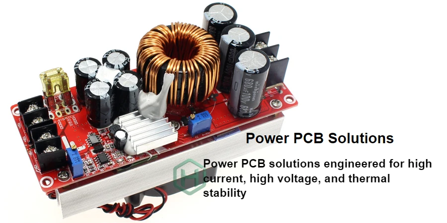
With the rapid growth of AI, data centers, 5G communications, and EVs, power density in electronic systems is rising faster than ever. From server racks to on-board charging modules, 48V architectures have become mainstream—bringing hard challenges in conversion efficiency and thermal management. Integrating high-efficiency power conversion and reliable cooling on a compact PCB is now a key determinant of product success. This is exactly where Turnkey PCBA delivers value: by unifying design, fabrication, and assembly, it provides a seamless path from concept to finished product and addresses the complexity created by high power density in a systematic way.
As an engineer focused on 48V power conversion, I know that a small layout mistake or a poor material choice can cause steep efficiency loss, thermal runaway, or even EMC compliance failure. This article explores how to use the Turnkey PCBA model to manage the key technical links in power and cooling systems, keeping your project on the right track from day one.
Turnkey PCBA: solving high-power-density problems at the design source
In traditional PCB development, design, fabrication, and assembly are often separated. Information gaps are common. When a “finished” design is sent to a factory, DFM (Design for Manufacturability) or DFA (Design for Assembly) issues often emerge—leading to expensive rework and schedule slips.
The Turnkey PCBA model changes this fundamentally. It emphasizes early collaboration between design engineers and manufacturing/assembly experts. In high-power PCB projects, this collaboration is especially valuable:
- Early risk identification: Manufacturing experts can evaluate risks such as heavy-copper etching, drilling high aspect-ratio vias, and soldering large components, then provide optimization suggestions during the design phase.
- Performance–cost balance: Co-select the best materials (e.g., high Tg laminates, low-loss dielectrics) and stackups to meet electrical/thermal requirements while controlling fabrication cost.
- Thermal integration: Consider thermal features (thermal-via arrays, embedded copper blocks) together with electrical placement to avoid late redesigns caused by insufficient cooling.
- Supply-chain optimization: A one-stop provider integrates component sourcing, PCB fabrication, and PCBA assembly—protecting quality and delivery, which is critical for emerging power devices such as GaN.
With this front-loaded, system approach, Turnkey PCBA removes many problems before they appear and builds a solid foundation for high-performance, high-reliability power and cooling systems.
High-efficiency power conversion core: 48V→12V/1V topologies and layout strategies
Data centers and automotive electronics widely use 48V buses to reduce I²R losses. But end loads (CPU, GPU, etc.) require voltages down to ~1V, creating huge demand for compact, high-efficiency DC-DC converters.
Topology selection: multi-phase interleaving and GaN
To handle hundreds of amps and achieve fast transient response, multi-phase interleaving buck converters are the standard. By splitting total current across multiple parallel phases and shifting their switching timing, you can:
- Reduce input/output ripple: lowering the required input/output capacitance.
- Increase effective switching frequency: shrinking passives (inductors/capacitors).
- Improve thermal distribution: spreading heat across the PCB and avoiding local hot spots.
In recent years, GaN power devices—thanks to extremely fast switching and low switching losses—have reshaped power design. Fully leveraging GaN performance places very high demands on PCB layout and is a key measure of GaN power stage PCB quality. Any solid GaN power stage PCB guide will emphasize minimizing parasitic inductance in the power loop.
Layout essentials: minimizing parasitics
In high-frequency switching applications, PCB traces are part of the circuit. A high-quality 48V to 12V conversion board layout must follow strict principles:
- Minimize power-loop area: Reducing the “Hot Loop” area is the top priority for suppressing voltage overshoot and EMI.
- Symmetric layout: In multi-phase designs, keep power paths and control-signal paths consistent in length and impedance to achieve accurate current share.
- Gate-drive optimization: Gate-drive loops must be as short and wide as possible and kept away from high-current paths to prevent noise coupling and false triggering.
Building a high-performance low-loss 48V to 12V conversion board is not only about component choice—it is also an art of layout.
Core principles for power-path layout
- Minimize the power loop: Place input capacitors, power switches, and bypass capacitors as close as possible to reduce high-frequency loop inductance.
- Split-ground strategy: Use separate power ground (PGND) and analog/signal ground (AGND), and connect them at a single point to prevent power-loop noise from contaminating control circuitry.
- Kelvin connections: Use Kelvin routing for current-sense resistors and voltage-feedback points so measurement accuracy is not affected by IR drop on high-current paths.
- Symmetry & current share: In multi-phase parallel designs, keep each phase layout mirrored/symmetric for balanced current distribution and thermal spreading.
PDN design: the foundation of stable power delivery
The goal of a Power Distribution Network (PDN) is to deliver stable, low-noise voltage under all operating conditions. For CPU/GPU loads with hundreds of amps of peak current, PDN design can make or break a system. The core is controlling PDN impedance within the target frequency band (Z-target).
PDN design typically includes three layers:
- VRM (Voltage Regulator Module): The source side, handling large, low-frequency load-current changes.
- PCB power/ground planes: Acting as board-level capacitance for mid-frequency charge storage.
- Decoupling capacitor network: Placed close to the load IC to provide high-frequency transient current and suppress SSN.
A robust PDN requires careful planning of capacitor values and packages (ESL/ESR) and strategic placement to maintain low impedance from DC up to hundreds of MHz.
Advanced thermal management: tradeoffs from air cooling to liquid cooling
All power loss becomes heat. If heat cannot be removed effectively, junction temperatures rise quickly, causing De-rating, reduced lifetime, and even permanent failure.
PCB-level thermal techniques
At the PCB level, you can strengthen cooling in several ways:
- Thermal vias: Dense arrays under power-device thermal pads conduct heat to backside heat-spreading layers or heatsinks.
- Copper pour: Large copper areas on inner/outer layers provide heat spreading paths.
- Heavy Copper PCB (Heavy Copper PCB): Using 3oz or thicker copper not only carries higher current but also conducts heat far better than standard 1oz. Learn more about HILPCB heavy copper PCB capability.
System-level cooling options
When PCB-level techniques cannot handle extreme heat flux, stronger system-level solutions are needed.
Cooling technology selection: comparison
| Cooling approach | Applicable power density | Advantages | Challenges |
|---|---|---|---|
| Forced air + heatsink | Medium/low (< 100 W/cm²) | Low cost, mature technology, high reliability | Large volume, noise, sensitive to ambient temperature |
| Heat pipe / vapor chamber | Medium/high (100-300 W/cm²) | Very high thermal efficiency; can transport heat over distance | Orientation/gravity effects; higher cost |
| Liquid cooling (Cold Plate) | High/ultra-high (> 300 W/cm²) | Best cooling capacity, low noise, compact system | System complexity, leak risk, high cost |
Materials and stackup: building the physical base of reliable power PCBs
Materials are the backbone of a PCB. Their properties directly affect electrical performance, thermal performance, and long-term reliability.
- High Tg materials: Tg (glass transition temperature) measures a laminate’s ability to maintain rigidity at elevated temperature. For areas near power devices where temperature may exceed 150°C, selecting materials with Tg ≥ 170°C (e.g., S1000-2M) is critical to prevent delamination or deformation during assembly and long-term operation. Learn more about high Tg PCB.
- Low-loss dielectrics: For high-frequency switching with GaN, dielectric loss (Df) affects SI and efficiency. Materials such as Megtron 6 or Tachyon 100G can significantly reduce high-frequency loss.
- Rigid-flex PCB: In compact power modules or cases that connect boards across planes, Rigid-flex PCB provides a high-integration solution. By combining rigid and flexible circuits, it eliminates connectors/cables, improving reliability and reducing size. In power applications, copper thickness and material choices in the flex section impose special requirements for current carrying and thermal performance.
DFM and DFA: ensuring GaN power-stage PCB quality and manufacturability
A design that is perfect on paper is worthless if it cannot be manufactured and assembled economically and reliably. This is why DFM and DFA matter.
Manufacturing challenges
- Heavy-copper etching: When etching 4oz or thicker copper, lateral undercut becomes more pronounced. Precise etch compensation is required to maintain trace-width accuracy.
- Thermal-via filling: To ensure pad flatness and soldering quality under components, thermal vias often require conductive/non-conductive resin plugging and surface metallization (POFV - Plated Over Filled Via).
- Warp control: Large, asymmetric copper distribution can cause warp during thermal processing and hurt SMT assembly. Optimized stackup and panelization can reduce warpage effectively.
Assembly challenges
- Soldering large thermal pads: Power devices (MOSFET, QFN ICs) often have large ground pads tied to inner heat-spreading copper. This makes soldering difficult. You must optimize the reflow profile to ensure full wetting while controlling voiding.
- Press-fit connectors: For Busbar connections carrying hundreds of amps, Press-fit connectors are often more reliable than soldering, offering lower contact resistance and stronger mechanical robustness.
Any detailed GaN power stage PCB guide must include these manufacturing and assembly considerations to ensure final GaN power stage PCB quality. Experienced manufacturers like HILPCB can engage early to provide professional DFM/DFA analysis.
HILPCB high-power PCB manufacturing capability
- ✓ Heavy copper capability: Supports up to 20oz heavy copper on inner and outer layers.
- ✓ High Tg material inventory: Stocked with high Tg, low-CTE materials such as S1000-2M, IT-180A, TU-872.
- ✓ Advanced thermal processes: Resin/copper-paste via filling, embedded copper blocks, metal-core boards (MCPCB), and more.
- ✓ Precision tolerance control: Tight control of line/space, impedance, and stackup thickness to meet demanding electrical performance requirements.
EMC/EMI and safety compliance: a system approach from layout to filtering
Switch-mode power supplies are strong EMI sources. Conducted and radiated noise not only affects other parts of the system but must also meet strict regulations (CISPR, FCC, etc.).
- At the layout level: Following good 48V to 12V conversion board layout practices is the foundation. This includes minimizing switching loops, using continuous ground planes, and isolating high-frequency and sensitive signals.
- Filter design: Proper LC filters at the input and output can suppress Differential-mode and Common-mode noise.
- Safety requirements: For power supplies connected to mains or high-voltage DC buses, creepage and clearance rules must be met to prevent electric shock and fire risk.
A qualified Turnkey PCBA provider must not only build boards, but also understand these system-level compliance requirements and support you throughout design and manufacturing.
HILPCB Turnkey PCBA: one-stop solution from prototype to mass production
Integrating electrical, thermal, mechanical, and manufacturing factors is difficult. This is exactly the value of HILPCB Turnkey PCBA: a one-stop solution covering engineering support, component sourcing, PCB fabrication, final assembly, and test.
Our strengths include:
- Deep expertise: Our engineering team specializes in power electronics and can optimize your design to build a true low-loss 48V to 12V conversion board.
- Flexible manufacturing: Heavy copper, Rigid-flex PCB, and high-frequency materials are all supported with high quality.
- Strict quality control: We understand GaN power stage PCB quality and use AOI, X-Ray, and functional test to ensure every assembly step meets high standards.
- Seamless project management: You work with a single project manager who controls the entire flow from design files to delivery, greatly simplifying supply-chain management.
Choosing HILPCB means choosing a partner that understands your technical challenges—and can deliver them reliably.
Common Questions
Why does turnkey PCBA help with high-power-density designs more than a fragmented supply chain?
High-power boards involve tightly coupled electrical, thermal, mechanical, and process decisions, so splitting responsibility across many vendors often slows feedback and hides root causes. A turnkey model shortens that loop by aligning design review, fabrication, assembly, and test under one engineering flow.
What should teams pay special attention to on GaN power-stage PCBs?
They need to manage copper thickness, thermal-via structure, warpage, large thermal pads, and connector strategy as one package. These factors directly affect switching efficiency, solderability, cooling performance, and long-term reliability, so they cannot be left to downstream manufacturing interpretation.
Why are EMC and safety compliance part of the manufacturing conversation?
Layout, filtering, creepage, clearance, and grounding choices are only useful if the final board is built exactly as intended and remains stable through assembly. Manufacturing capability therefore has to support the compliance strategy rather than merely reproduce geometry from Gerber files.
Conclusion
Power and cooling system PCB design and manufacturing is an art of balancing electrical, thermal, and mechanical constraints. As power density rises, traditional fragmented development models are no longer sufficient. Turnkey PCBA integrates the expertise of design, fabrication, and assembly from the start through an integrated, collaborative workflow—systematically solving layout, thermal, material, and process challenges driven by high power density.
To manage this complexity, you need more than advanced components—you need a strong partner that can translate design intent into a high-reliability product. Choosing an experienced Turnkey PCBA provider like HILPCB is a smart way to accelerate time to market and maintain competitiveness.